RESEARCH AREAS
BULK, SINGLE CRYSTAL GROWTH
Ammonothermal Method
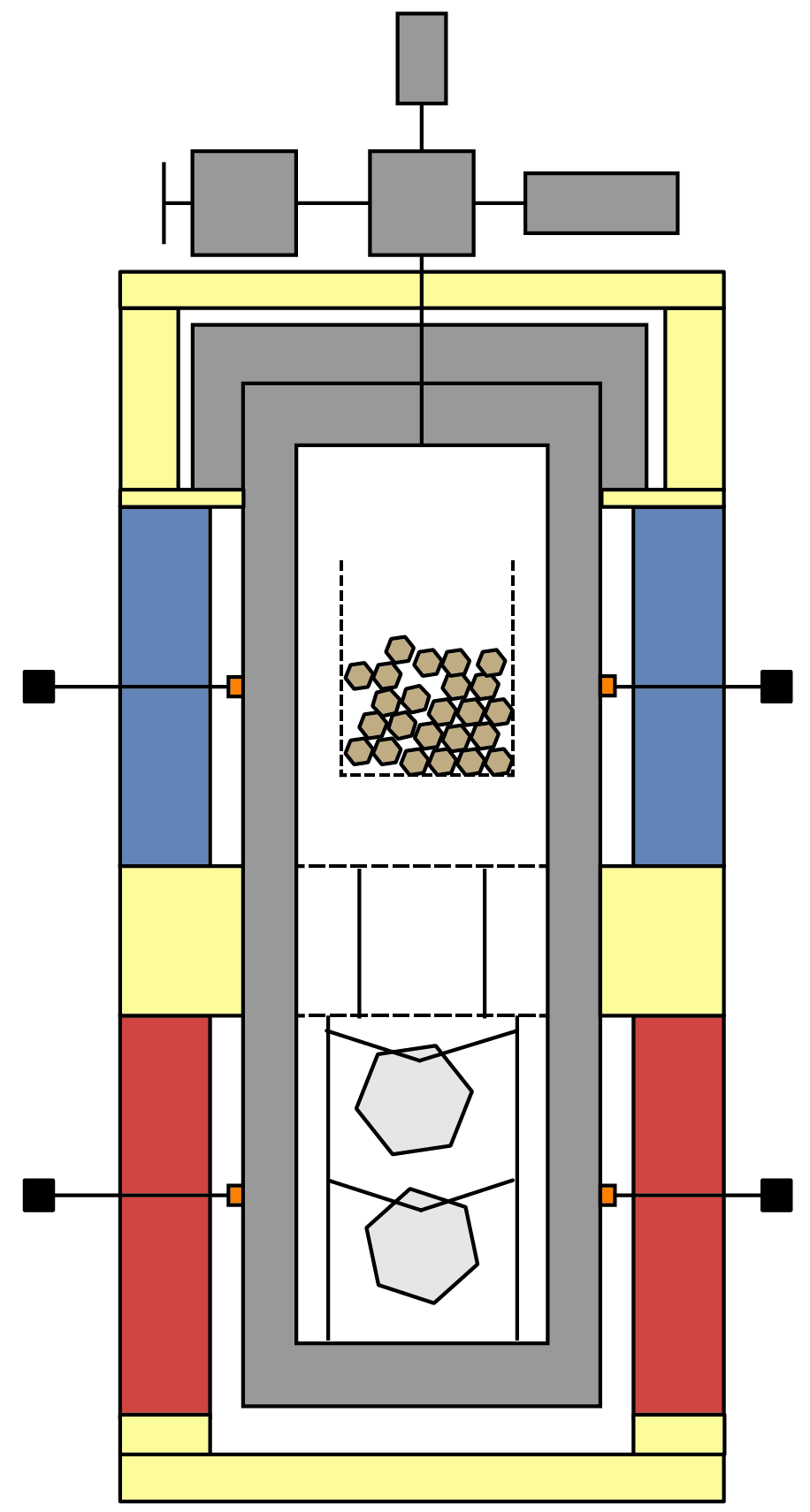
The ammonothermal method uses supercritical ammonia to dissolve and crystalize a variety of nitride materials. Due to the propensity for nitride materials to decompose at elevated temperatures, this process is ideally suited as it combines high pressure (activity) nitrogen with low growth temperatures enabling growth of novel nitrogen-containing materials. Using this method, a variety of technologically and scientifically interesting compounds can be grown. Some materials of current interest include:


While the method has been demonstrated on an industrial scale, much remains to be explored on the fundamental level to aid in our understanding of the underpins of the method and help with developing accurate models to improve on yield and performance of this method. Topics include equilibrium properties, such as solubility, equation of state development for NH3-N2-H2-O2 systems and decomposition of ammonia.
Keywords: Ammonothermal, Bulk Crystal, Single Crystal, Gallium Nitride, Boron Nitride, Indium Nitride, Oxy-nitride, Solubility, Thermodynamics, Equation of State, Decomposition of Ammonia, Corrosion, Autoclave, Nickel Chromium Superalloys, Titanium Zirconium Molybdenum
Flux-based Methods
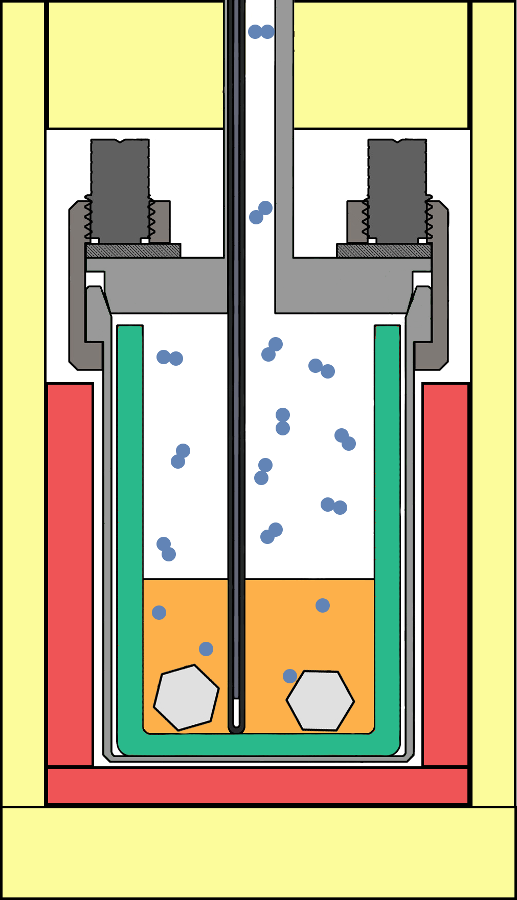
In many scenarios, growth of novel materials requires the use of a specially tailored growth environment to take advantage of thermodynamics and the ability to properly dissolve the desired constituents of the growing crystal. For nitrides, the challenges are compounded by the need to dissolve nitrogen into a molten metal solution. Alkali metals are prime candidates as flux materials, though have a high vapor pressure requiring the development of a unique system to properly contain the vapor while allowing transport of nitrogen gas into the system. Using this novel approach, the bulk growth of ternary nitrides and growth of hexagonal boron nitride is of interest to investigate material properties and provide substrate materials for future device development.


Keywords: High-Pressure Flux Growth, Solution Growth, Alkali Metal, Ternary Nitrides, Indium Gallium Nitride, Aluminum Gallium Nitride, Aluminum Indium Nitride, hexagonal Boron Nitride, Perovskites, in situ monitoring, Thermodynamics
THIN FILM GROWTH
High Pressure Chemical Vapor Deposition (CVD)

Fabrication of (opto-)electronic devices typically requires the use of a thin-film based growth technique to tailor material compositions with an atomic level precision. To provide sufficient energy for atoms to diffuse on the surface of the growing material, elevated temperatures are needed. This presents a fundamental challenge for decomposition-limited materials, such as indium-containing Group III-Nitride materials. A consequence is the inability to grow crystals with high indium content, limiting access to desired material properties. One approach to overcome this challenge is to design and develop a thin-film growth tool that can operate at high pressure (up to 100 atm!). This work is ground-breaking as the tool design overcomes known challenges related to high-pressure thin-film deposition techniques and promises to grow high-indium content Group III-Nitride (full composition range from 0-100%) along with oxy-nitrides and possibly high-pressure phases such as cubic boron nitride.


Keywords: High Pressure, Chemical Vapor Deposition, Thin Film, Single Crystal, High Indium, Group-III Nitride, Indium Gallium Nitride, Aluminum Indium Nitride, Oxy-Nitride, cubic Boron Nitride, Kinetics, Thermodynamics, Computational Fluid Dynamics, Heat and Mass Transfer, Equipment Development
DEVICE DEMONSTRATIONS
Power Electronics

Electricity generation accounts for ~ 40% of the primary energy consumption in the U.S. and is projected to increase to more than 50% worldwide. The fraction of energy processed through some form of power electronics will be as high as 80% in 2030. The development of advanced power electronic devices with exceptional efficiency, reliability and functionality are critical. This group focuses on the development of novel materials for the purpose of fabricating the next-generation power electronic devices. Of particular focus is cubic boron nitride as it can be both p- and n-type doped while exhibiting a superior figure of merits compared to other power electronic materials being pursued today, including diamond.

Keywords: Power Electronics, Wide Bandgap Semiconductors, High Voltage Devices, Breakdown Voltage, cubic Boron Nitride
Optical Absorber and Emitters

While exceptional progress has been made towards inexpensive visible light emitters and solar cells, much works remains in enabling high efficiency, high power UV light emitters for disinfection purposes and earth-abundant solar cell absorbers for improving on the overall efficiency of solar cells and their use in (photo)electrochemical systems for water splitting or disinfection applications. By taking advantage of perfectly lattice matched, ternary nitride substrates high-efficiency UV emitters are being pursued. Use of novel oxy-nitride materials in photoelectrochemical and solar absorber systems is being investigated.


Keywords: LEDs, Lasers, Solar Cells, Photoelectrochemistry, Water Splitting, Earth-abundant elements
