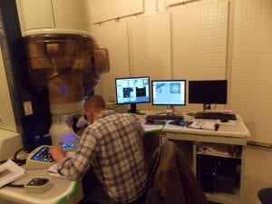
The instrument is a JEOL ARM200CF, it is located in Whitaker Laboratory room WH178A. The room is specially adapted to provide the necessary stability of temperature without a large airflow by means of cold water filled panels (seen in the photograph below).
The Atomic Resolution Microscope (ARM) really does allow us to image atoms, singly or in groups on ultra-thin substrates – or picture arrays of atoms, in crystals of various sizes with ultimate resolution below 0.1 nm. Several focused probes sizes can analyze nanoparticles down to 1.0 nm in size and still provide sufficient beam current to excite plenty of X-rays.
- Combined with very sensitive JEOL X-ray collection technology this is our most powerful analytical tool, capable of detecting a single layer of atoms segregated to grain boundaries.
- The scanning electronics are driven by a Gatan DigiScan 2 system that interfaces with a Thermo Electron data acquisition EDS computer.
- The electron source is a cold field emission system with outstanding beam current stability. Operating voltages range from 60 to 200 kV.
- The aberration corrector (CEOS ASCOR) is of fourth order and allows a wide angle of convergence (e.g. 32 mrad.) to electrons arriving at the sample; this is key to high beam current and small probe size.
- As a TEM the instrument is also very good and features a cooled CCD camera (Gatan UltraScan 1000), we have software to help correct alignment through Digital Micrograph (Gatan).
- We have a Hummingbird Scientific tomography specimen holder and access to a Protochips Aduro double-tilt heating holder owned by Professor Martin P. Harmer’s research group.
- We are a partner in the Nano Human Interface initiative (https://www1.lehigh.edu/file/nano-human-interfaces-initiative)
- We have a noise cancellation device fitted to remove “tip noise”.
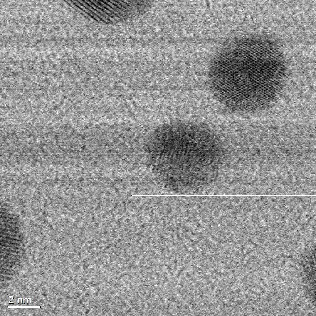
A bright field STEM image showing the effects of the Noise cancellation device (switched on just over halfway down the frame). Cold field emission sources build up layers of adsorbed gases over time that cause instability in the emitted current; these instabilities manifest themselves as horizontal streaks or bands in the image.
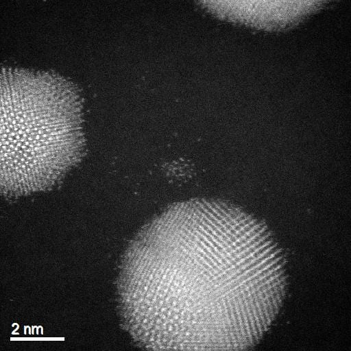
Single atoms of gold are imaged via the technique of high angle annular dark field (HAADF) STEM; the atoms are bright dots found between the nanoparticles on the thin carbon support material (likely between 3 and 5 nm thick). The atomic number contrast between gold and carbon is most evident in this type of “Z-contrast” image.
Contact: rok210@lehigh.edu
Powered by Simple Calendar
April 2024
Mon
Tue
Wed
Thu
Fri
Sat
Sun