Research Facilities and Equipments – Lehigh University (Tansu Group)
Lehigh University has unveiled a 2020 Plan to strengthen its research nucleus. The expansion of the Electrical and Computer Engineering (ECE) is one of the major thrusts within that initiative. Increased focus in the research and development of Optoelectronics, Photonics, Nanotechnology, Optical Communications, and Information Technologies are the key pillars to this growth. Within the recently-established Center for Optical Technologies (COT), Lehigh invested in some of the state-of-the-art III-V semiconductor MOCVD epitaxy and device fabrication cleanroom facilities, to address the high-end optical and optoelectronic device fabrication and integration needs. An entirely new ~12,000 ft2 four-story building (Smith Family Laboratory for Optical Technologies), has been dedicated for the MOCVD epitaxy and III-V device fabrication. This new $6.5M facility is paid through Lehigh’s internal funds and generous alumni support. One entire floor of this new facility is dedicated to MOCVD research led by the PI. The pro-rated funds allocated by Lehigh to the PI’s research program alone exceed ~$1.5M. These are used to acquire research equipments such as the two MOCVD reactors. The new facility is streamlined for research in the fields of semiconductor nanostructure, semiconductor optoelectronics, photonics integrated circuits, and III-Nitride / III-V semiconductor devices. Other capabilities to support the optoelectronics devices include, extensive material and structural characterization, device testing, and computational resources. All these capabilities are discussed further below.
III-V Semiconductor MOCVD Epitaxy Facility
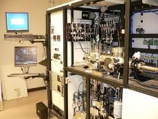
Smith Laboratory houses the PI’s new MOCVD lab facility. The two MOCVD reactors are VEECO P-75 and VEECO D-125, for III-Nitride and GaAs/InP research, respectively.
VEECO P-75 GaN based MOCVD Reactor (PI’s Lab)
 The P-75 MOCVD reactor provides us capabilities to pursue research on AlInGaN materials and devices for optoelectronics and nanostructures. The reactor is equipped with 6 metalorganic sources (TMIn, TMGa, TEGa, TMAl, and Cp2Mg), and is capable of growing compound semiconductor materials containing In, Ga, Al, and N. Dopant species of Mg and Si are available for device applications. The P-75 reactor is also used to pursue research on low-cost and compact deep-UV light sources using AlInGaN semiconductor nanostructures, efficient white-light LEDs, InGaN semiconductor nanostructure optoelectronics, GaN-based electronics devices, and InN-based semiconductor thin film and nanostructures. A new line for Cr-/Mn-precursor has also been installed for pursuing III-Nitride spintronics materials.
The P-75 reactor is also equipped with RealTemp® in-situ instrumentation, which allows real-time correction of emissivity during epitaxial deposition, to give reliable and repeatable temperature readings. The utilization of RealTemp® enables us to determine extremely accurate growth rates, to conduct quantitative analyses of buffer layers, and to estimate the composition of ternary and quaternary materials. Because of the high degree of repeatability from one run to the next, the PI’s group is able to focus on making small adjustments needed to closely examine the novel compound semiconductor materials and ultimately improve our epi results.
VEECO D-125 GaAs/InP based MOCVD Reactor (PI’s Lab)
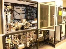 The D-125 MOCVD system is dedicated for optoelectronics and nanostructure research on GaAs/InP substrates. The D-125 MOCVD reactor has been customized for 12 metalorganic sources (2 TMGa, 2 TMIn, 2 TMAl, TMSb, UDMhy, TBP, TBA, DEZn, and CBr4), which allows the versatile growth of novel and new semiconductor material system. The reactor is capable to grow compound semiconductor materials containing In, Ga, Al, As, P, Sb, and N. Elements of Zn, C, and Si are also available in D-125 reactor for doping purposes. The D-125 reactor is also used to grow dilute-nitride and Sb-based semiconductor nanostructure optoelectronics devices, quantum dots lasers and amplifiers, interdiffused quantum dots, solar cell, and terahertz sources. The D-125 is also equipped with in-situ RealTemp® instrument.
III-V Semiconductor Characterization Facility
In addition to the III-V epitaxy capabilities, extensive material characterization facilities are available in Smith Laboratory, including Hall measurements, optical reflectance, photoluminescence mapper, X-Ray diffractometer, atomic force microscopy (AFMs are available in material science engineering department at Lehigh), confocal and scanning near-field optical microscopy (confocal and NSOM are available in Physics Department at Lehigh).
Philips PLM-100 Photoluminescence mapper (PI’s Lab)
The PLM-100 is a versatile screening tool, producing high resolution maps of compound semiconductor epitaxial wafers that make variations in layer composition, quality or thickness visible. It provides the PI and his group with reliable feedback needed to optimize the growth processes. It also gives valuable information on a wafer’s projected device yield. Screening wafers helps to ensure a supply of high quality and high uniformity epilayers required efficient processing.
Bede Scientific QC2a X-Ray Diffractometer (PI’s Lab)
The QC2a has five motorized axes on the sample stage and extended angular range, allowing access to asymmetric reflections for the measurement of relaxed systems and samples with highly misoriented substrates. The QC2a uses double crystal X-ray diffraction to remove the divergence characteristics of the X-ray beam from a 60W air cooled X-ray source. Reference crystals are mounted in interchangeable, pre-aligned beam conditioner blocks, which are selected to match the substrate material of the specimen being analyzed. It can perform high resolution X-ray diffraction on a variety of compound semiconductor materials.
Bio-Rad HL 5200 Hall Measurement System (PI’s Lab)
The HL 5200 provides for the measurement of net carrier concentration and carrier mobility via the van der Pauw Hall analysis. HL 5200 is fully computer controlled and equipped with software to verify contact ohmicity over the measurement current range and to calculate van der Pauw statistics for the measurement. This system has been can be used on a variety of compound semiconductor materials.
Confocal Luminescence Microscope (Physics Department)
 The confocal luminescence microscope is a specially developed in-house system, and it is capable of conducting the optical luminescence measurement from low temperature (T=~10K) up to room temperature. It is a completely fiber-based set up. The output and the input of the single mode fibers replace the usually required pinholes and allow a light and compact design of the instrument, allowing the motion of the whole microscope without sacrificing speed. Different from most commercial instruments, which record only the emission intensity, the in-house system is able to acquire a whole spectrum for each spatial position.
WiTec AlphaSNOM Scanning Near-field Optical Microscope (Physics Department)
 The design of the Alpha-SNOM features a Confocal Microscope (CM), a Scanning Near-Field Optical Microscope (SNOM) and an Atomic Force Microscope (AFM) in a single instrument. SNOM allows optical microscopy with highest spatial resolution beyond the diffraction limit. The AlphaSNOM uses an extremely precise capacitively-controlled piezo platform to scan the sample in three dimensions. The stage is used not only in SNOM and AFM, but also in confocal mode. Therefore, it is possible to analyze the same sample area with different techniques and combine the benefits of all three modes.
Structural Materials Characterization Facility – Electron Microscopy
 The Nanocharacterization Laboratory at Lehigh contains the largest electron microscopy laboratory in the U.S., with a suite of 12 scanning, transmission and scanning / transmission instruments. These are well suited for characterizing nanoscale structures and chemistry via an unparalleled range of imaging and analytical methods. The Electron Microscopy facility has excellent supporting services to keep the instruments at peak performance and to optimize their use. There are complete specimen preparation facilities including a Gatan PIP’s, a plasma cleaner, chemical jet polishers, dimplers, wire saws, diamond cutting wheels and a comprehensive metallographic suite. In addition, there are dark rooms, facilities for digital image acquisition and manipulation, off-line computers for data analysis, and extensive microscopy-related software. Modifications to the instruments can be developed with the aid of a machine shop which is nearby. The Nanocharacterization Laboratory houses the world’s highest resolution X-ray analytical microscope – a unique instrument custom designed for nanoscale analysis and imaging. By taking advantage of the excellent facility and tremendous knowledge on electron microscopy laboratory at Lehigh, we plan to utilize this facility for characterizing our semiconductor nanostructure/optoelectronics devices (ie. TEM for quantum wells/dots, SEM for optoelectronics devices structures, and others).
III-V Semiconductor Cleanroom Fabrication Facility
The Smith Family Laboratory for Optical Technologies also has a new III-V semiconductor university-shared cleanroom facility. The cleanroom facility supports research and developments in microfabrication techniques, and device fabrications. All the semiconductor optoelectronic materials grown in the PI’s MOCVD laboratory will be fabricated into devices in this new cleanroom facility. The cleanroom facility include photo-lithography (Karl Suss MA-6), intermixing/contact annealing (RTA), III-V and dielectric etchers (ICP and RIE), SiO2 and Si3N4 deposition (PECVD), metallization and AR/HR (e-beam evaporator and sputterer), holography system (grating formation for DFB/DBR lasers), wet etching, wafer thinning, laser scribing, and basic laser packaging.
A new electron-beam lithography system is available for use in the Sherman Fairchild Center for Solid-State Studies (Director: Prof. Marvin H. White). A versatile Focused Ion Beam (FIB) instrument, which is useful for realization for nanofabrication of photonic crystals and optoelectronic devices, is also available in Lehigh’s Center for Advanced Materials and Nanotechnology.
Optoelectronics Devices Testing and Semiconductor Characterization Facility
The laser diode testing facility in PI’s lab at Lehigh’s Center for Optical Technologies allows measurements of DC and AC characteristics of laser devices and LEDs. The facilities here allow measurements of the pulsed laser P-I, continuous-wave laser P-I, device I-V characteristics, absorption loss measurements, optical gain and alpha-parameters measurements, and high-speed measurements. Complete photodetector characterization can also be conducted at Lehigh’s COT. A new Keithley 2520 pulsed laser diode set up and Labsphere integrating sphere (with Ge and strained Si detectors) also allow accurate pulsed laser / LEDs testing (with temperature range from 5 oC up to 100 oC) from wavelengths of 200nm to 1800nm. This testing facility allows measurements of basic characteristics of optoelectronics devices, as well as extractions of physical parameters essential for further understanding and optimization of devices.
New testing set up for solar cells is available in PI’s lab at Lehigh’s Center for Optical Technologies. The new solar cell measurement set up allows measurements of open voltage and short-circuit current, and efficiency of solar cells fabricated in PI’s lab. The solar cell measurement set up include I-V testing equiptment (Agilent U2722A), solar simulator (ABET 150 Watt Xenon Arc Lamp with AM 1.5G Filter), and reference cell. Thermoelectric test measurement set up is available in PI’s at Lehigh. The thermoelectric set up available in PI’s lab allow simultaneous measurements of electrical conductivity, thermal conductivity, and Seebeck coefficients. The measurement of thermal conductivity of material is conducted by using 3- method.
Computational Resources
 The computation capabilities for various aspects of semiconductor optoelectronics and semiconductor nanostructure devices are available in the PI’s lab at Lehigh. Many advanced computational techniques on the physics of semiconductor nanostructure and photonic device design are developed in-house by the PI and the students. They include but not limited to, programs to simulate and design optoelectronics devices, vertical cavity surface emitting lasers, solar cells, thermoelectric materials, carrier transport, thermionic emission of carriers, quantum well/dot intermixing process, band structure and optical gain of semiconductor nanostructure, and others. Advanced photonic computational techniques for photonic crystals, 2-D and 3-D complex optical waveguide, integrated optics, and finite-difference time-domain analysis are also developed in-house in PI’s lab. The PI and his group also have access to Lehigh’s SGI Altix 350 supercomputer, which is a symmetric multiprocessor (SMP) machine consisting of 32 CPUs, 128 GB of shared memory and 1 TB of hard disk capacity. Numerical models based on technology computer aided design (TCAD) is also available for accurate modeling of III-Nitride and III-V semiconductor optoelectronics devices. The numerical model takes into considerations the electrical, optical, and thermal effects in simulating the device structures. In particular, the numerical models include models for carrier and heat transport, quantum effects, heterostructures, carrier capture in QW, band structures, spontaneous emission and optical gain simulations, and full-wave solutions of the Maxwell equations to account for physical optics in advanced devices.