Biophotonics: Sensing and Imaging
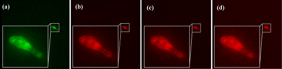
 While fluorescence microscopy is a powerful and well-established technique, it typically requires bulky, expensive instrumentation, and consequently is not suitable for widespread use or for the concurrent measurement of many samples. Recent advances in nanofabrication, however, now make it possible to consider complete systems on a chip. Such miniaturization has the potential to achieve orders of magnitude reduction in cost, size, and processing time, but significant challenges remain if full functionality on a chip is to be achieved at the required performance levels.
 Integrated nanophotonic systems for fluorescence sensing and bioimaging are very promising for health care, biomedicine, biosensing, and environmental monitoring applications that require low cost, compact size, and a capability for high-throughput screening. This multidisciplinary research address significant challenges in micro-optical design and component miniaturization that must be overcome to realize such systems (see Publications [6]).
Nanophotonics: Plasmonics
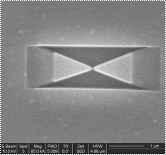
 Plasmonic structures and devices operating at optical frequencies have interesting applications such as on-chip integration of optical circuits, surface or interface technology, data storage, and bio-sensing. What makes the plasmonic structure unique is its potential for spatial confinement of electromagnetic (EM) energy within subwavelength dimensions over a wide spectral range. This occurs through the excitation of surface plasmon polaritons (SPP), which offer an attractive approach to overcome the size limitation that diffraction imposes on conventional photonic structures.
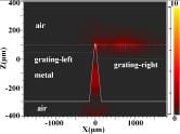
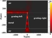
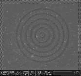 What has been missing until very recently is an effective method for ensuring that the generated SPPs travel only in the desired directions from the subwavelength launching point. Recently, we numerically demonstrated that two surface waveguide structures placed on the opposite sides of a slit can be introduced to confine and to guide light of different frequencies in opposite directions. Such structures, which are under continuing investigation, should be able to operate at frequencies ranging from the visible to THz domains. The grating structures can function not only as a DBR reflector for one wavelength but also as an effective waveguide for the other wavelength (see Publications [1,2,5]).
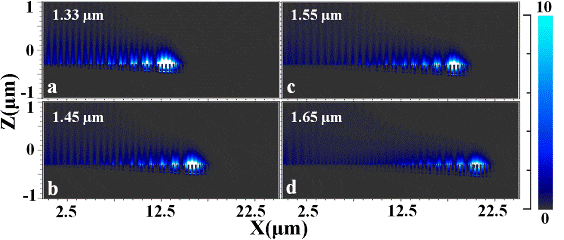
 As can be seen from their dispersion relations, SPP modes have the potential to produce slow light, i.e. EM waves with lower group and phase velocities compared to the corresponding free-space values. While promising steps have been taken towards slowing light in solid-state media and semiconductor nanostructures operating at room temperature, it still remains a great challenge to “stop” the light completely and implement such schemes on-a-chip incorporating optoelectronic devices. Recent reports of “trapped rainbow” storage of THz light in metamaterials and plasmonic graded-grating structures suggest a means to overcome these limitations and offer an attractive new way to stop light, making it possible to reduce the speed of the light over a wide spectral band, and operate at arbitrary temperatures (including room temperature)(see Publications [3,4,7]).