Research Works and Projects
Lehigh MOCVD and NanoPhotonics Group – Laboratory for Emerging Photonics & Nanostructures
“Advancing Nanotechnology for Energy, Communications, and Biotechnology”
Research Projects / Works (Click here for PDF format)
I. Research Areas / Interests and Background
Our research areas cover both the theoretical / computational and experimental aspects of the physics of semiconductor optoelectronics materials and devices & the physics of semiconductor nanostructure (quantum dots and quantum wells) and nanophotonics, based on Group III-Nitride (AlInGaN) and III-V-Nitride (InGaAsN) semiconductors. The experimental aspects include the material epitaxy with metalorganic chemical vapor deposition (MOCVD) & device fabrications of III-Nitride and III-V-Nitride semiconductor optoelectronics devices. The device applications addressed in our research include semiconductor light emitting diodes (LEDs) and solar cells for energy applications, and semiconductor lasers for biomedical and communication applications. Our research field, which is in the Applied Physics and Electrical Engineering areas, utilizes knowledge and ideas derived from fundamental physics to advance the science and technology of semiconductor optoelectronics for engineering applications. The fundamental physics cover knowledge of quantum mechanics, quantum electronics / optics, solid state physics, semiconductor physics, and electromagnetic, and we utilize these knowledge to solve problems related to the device physics of semiconductor nanostructures and optoelectronics. In our laboratory (as part of Center for Optical Technologies), we currently have two MOCVD reactors, with one reactor dedicated for the III-Nitride (GaN-based) optoelectronics and nanostructures research (P-75 reactor) and the other for GaAs / InP-based optoelectronics and nanostructures research (D-125 reactor).
The focuses of our research works include applications for energy (high-efficiency solid state lightings, solar photovoltaic cells, thermoelectric materials, and visible lasers), surface plasmonic devices, biological and chemical sensors (deep UV and THz optoelectronics), and communications (UV and InGaAsN-based LEDs / lasers). Our research works are funded by US National Science Foundation (NSF) [ECCS – 2 programs, DMR – 2 programs, CBET – 1 program, and SNM – 1 program], US Department of Energy (DOE) – 2 programs, DARPA – 1 program, US Department of Defense (DOD), Pennsylvania Infrastructure and Technology, and State of Pennsylvania.
II. Research Philosophy / Methodologies
In the pursuit of our research ideas, our research group strongly emphasizes on the integrated training of research and education for graduate students to achieve a strong understanding and expertise in both the theoretical and experimental aspects of their research works. In our group, all PhD students are expected to excel in both theoretical and experimental research. The theoretical topics are of great importance for enabling graduate students to deepen the fundamental understanding of the research topics. The experimental topics pursued by our PhD students primarily focused on the fields of MOCVD epitaxy, semiconductor / photonics device fabrication and physics, nanostructures and devices, surface plasmonc devices, solar hydrogen, and thermoelectricity. The purpose of this rigorous graduate training for the graduate students is to ensure high quality Lehigh PhD graduates in the field of semiconductor nanostructure and optoelectronics, who would have strong fundamental physics knowledge as well as the ability to apply this on technological problems.
Currently, our graduate students and postdoctoral researchers are equipped to conduct all the research works internally at Lehigh. These research works include: computational / theoretical design, material epitaxy, material characterization, device fabrications, and device characterizations and analysis. In addition to the facility described above (MOCVD, cleanroom fabrication, device characterizations, and material characterizations), our research group have also recently added new equipments enabling the following tasks:
1) thermoelectric and thermal conductivity characterizations,
2) solar cells and solar hydrogen measurements,
3) colloidal lithography process, and
4) phosphor synthesis facility for white LEDs project. The ability to perform all steps of the research works internally allow more efficient and effective research progress in our graduate students and postdoctoral fellows.
III. Broad Description on Research Topics / Works
Our research group has actively worked on the fields of semiconductor nanostructure and optoelectronics, focusing on the materials and devices for optical communications, solid state lightings, solar cells, THz optoelectronics and thermoelectric applications. As of January 2012, our research works have resulted in 81+ refereed journal publications (72+ published at Lehigh) and 150+ refereed conference publications (134+ published at Lehigh). Several additional new works are currently under-going in our laboratory. All these works focuses primarily on dilute-nitride semiconductor nanostructure gain media for near-IR and mid-IR lasers, III-Nitride semiconductor nanostructures LEDs / lasers for solid state lighting, III-Nitride-based solar cells, photonics devices for optical communications and high-power lasers, III-Nitride based thermoelectric materials and devices, III-Nitride semiconductor for solar hydrogen, and III-Nitride based terahertz photonics.
IV. Past Research Works – PhD Studies at University of Wisconsin-Madison (09/1998-05/2003)
My past PhD research works at the University of Wisconsin-Madison (under Prof. Luke J. Mawst) focused on the MOCVD epitaxy, device fabrications, and device physics of 1) 850-nm Al-free compressively-strained InGaAsP QW vertical-cavity surface emitting lasers (VCSELs), and 2) 1300-1550 nm strain-compensated InGaAsN QW lasers on GaAs substrates.
(i) Epitaxy and Device Fabrications of 850-nm Compressively-Strained InGaAsP QW VCSELs (09/1998-12/1999)
The goal of this project is to develop the compressively-strained InGaAsP QW VCSELs at λ=850 nm. The use of the compressively-strained InGaAsP QW for λ=850nm, is predicted theoretically to lead to a strain-induced reduction in the threshold and transparency current density of the lasers. Highly-temperature-insensitive compressively-strained InGaAsP QW, =850 nm, diode lasers have also been demonstrated for the first time, as part of the works performed in this project. The utilization of the InGaAsP QW is also expected to improve device reliability due to the existence of indium in the QW, which has been shown to inhibit dark-line defect propagation. As part of this work, λ=850 nm emitting VCSELs utilizing the compressively-strained InGaAsP QW have also been demonstrated for the first time.

Selected Relevant Publications
- N. Tansu, S. Rusli, D. Zhou, and L. J. Mawst, “Compressively Strained InGaAsP-Active (λ=0.78-0.85-μm) regions for VCSELs,” in Proc. of 12th IEEE Laser and Electro-Optics Society Meeting 1999, paper WA5, pp. 397-398, San Francisco, CA, Nov 1999.
- N. Tansu, D. Zhou, and L. J. Mawst, “Low Temperature Sensitive, Compressively-Strained InGaAsP Active (λ=0.78-0.85-μm) Region Diode Lasers,” IEEE Photon. Technol. Lett., Vol.12(6), pp.603-605 , June 2000.
- N. Tansu, and L. J. Mawst, “Compressively-Strained InGaAsP-Active (λ=0.78-0.85-μm) regions VCSELs,” in Proc. of the 13th IEEE Laser and Electro-Optics Society Meeting 2000, paper ThF2, pp. 724-725, Rio Grande, Puerto Rico, Nov. 2000.
(ii) Narrow Lateral Waveguide Single Mode VCSELs and Computational FDTD VCSELs
We proposed a novel approach for achieving high power single mode VCSELs, by using the concept of narrow lateral waveguide. The use of this concept allows one to achieve a large near field spot size for VCSELs structure. A narrow-waveguide VCSEL design incorporating a separate current confinement aperture is analyzed. This design then allows one to adjust the optical overlap with the gain region by choosing the current aperture. The device is fabricated by two-step MOCVD growth. The analysis of its modal properties is done by employing a full-wave FDTD simulation, for extracting the optical field profiles and cavity Q. Due to the nature of the narrow waveguide, only a single-spatial single mode is supported.
The novel idea of narrow lateral waveguide is also applied into edge emitting lasers (US Patent No. 6,845,116). This approach is regarding a new method to achieve high power edge-emitting semiconductor lasers by utilizing the novel ‘narrow lateral waveguide semiconductor lasers’. Often times, the maximum optical lasing power achievable from semiconductor lasers is limited by the high optical power density that damage the facet of the semiconductor lasers (due to the high optical power density at the output facet; typically high optical power density at the facet will melt the semiconductor facet, which would lead to catastrophic optical mirror damage of the diode lasers). The invention shows that by utilizing the ‘narrow lateral waveguide’ approach, one can spread the optical lasing mode field over a very wide (extremely wide) region thus leading toward lower optical power density at the output facet of the semiconductor lasers, which in turn will lead to higher maximum optical power achievable from the diode lasers (as the power density at the facet is lower, then higher maximum power can then be achievable before the laser facet will melt). The spreading of the optical mode of the diode laser based on this invention is achievable while maintaining the single mode operation throughout the whole lasing operation. The proposed method in this invention can also be grown by standard III-V semiconductor MOCVD / MBE epitaxy, and the device structures can also be fabricated by utilizing the standard semiconductor processing technology.
Selected Relevant Publicatons
- D. Zhou, T. W. Lee, N. Tansu, S. C. Hagness, and L. J. Mawst, “Large Spot Size Narrow Waveguide VCSELs,” in Proc. of the 14th IEEE Laser and Electro-Optics Society (LEOS) Annual Meeting 2001, San Diego, CA, Nov. 2001.
- Luke J. Mawst, Nelson Tansu, and et.al., “Narrow Lateral Waveguide Lasers,” Novel techniques to achieve high power single mode edge emitting lasers, US Patent No. 6,845,116; approved on January 18th 2005.
(iii) Strain-Compensated 1200-1400 nm InGaAsN Quantum Wells Lasers (01/2000-06/2003)
High-performance 1300-nm diode lasers capable of high temperature operation lead to low-cost (uncooled) transmitters applicable for optical communication, without the need of additional electronics to maintain thermal stability. The ease in forming high quality GaAs/AlAs distributed Bragg reflectors on GaAs substrates for VCSELs devices is also a major driving force for the development of 1300-nm diode lasers on GaAs. The pursuit of long-wavelength lasers on GaAs had been a very important topic in the early 2000s, due to its potential for forming band-offset QW-barrier heterostructure and the ease in implementation for VCSELs structures. Prior to 2001, the best-reported 1300-nm InGaAsN QW lasers have been realized with molecular-beam-epitaxy (MBE), resulting in performances superior to those by MOCVD. Our MOCVD-grown 1300-nm InGaAsN QW lasers were among the first to result in better threshold current density over that of MBE-grown devices, and the results were published in April 2002.
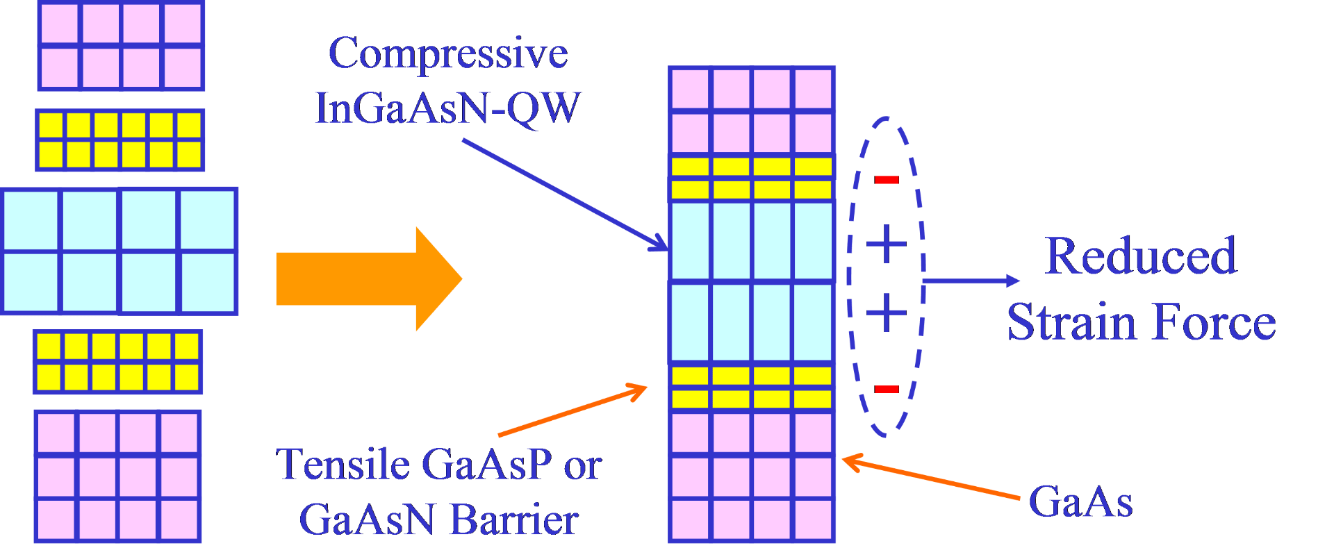


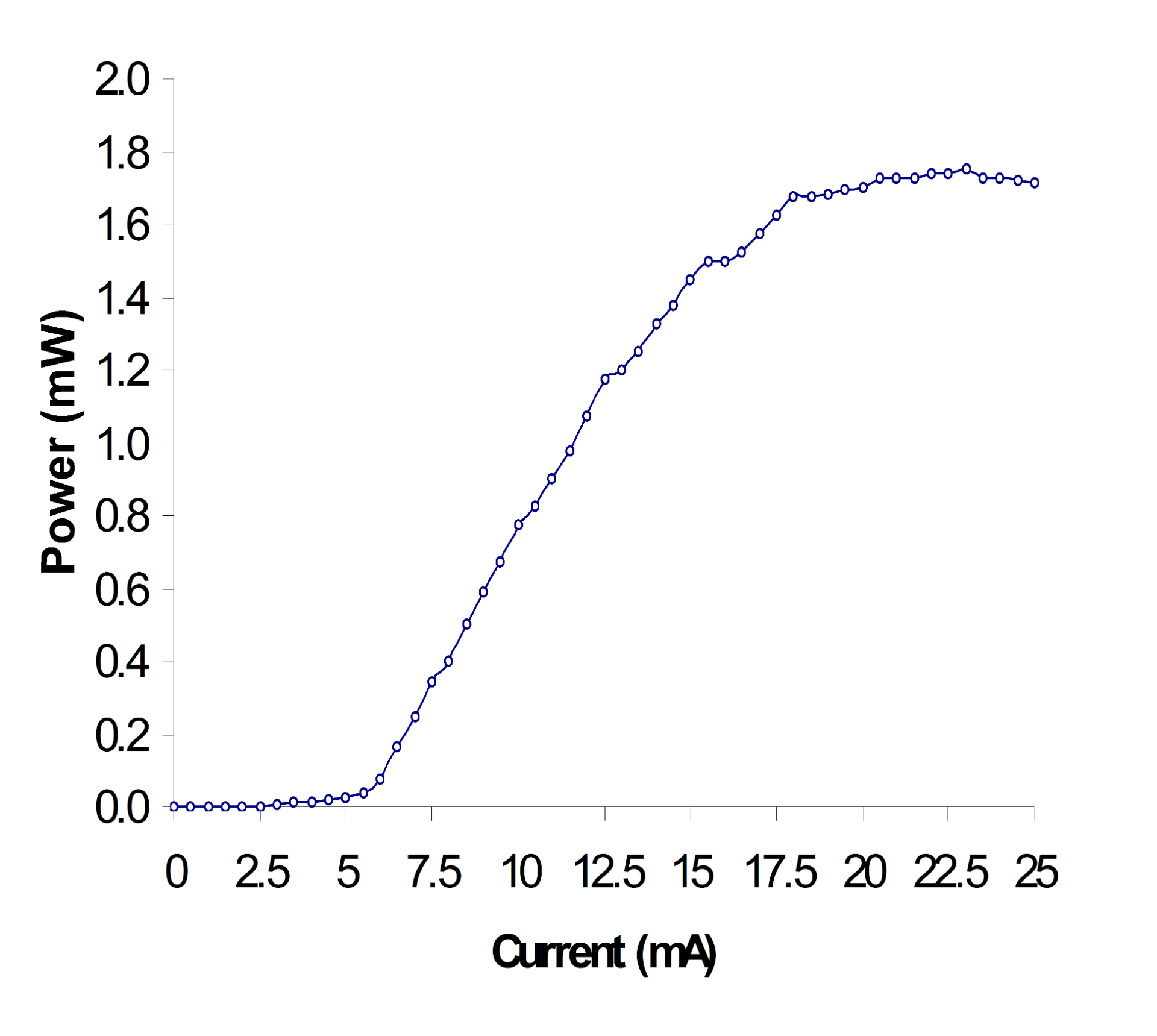
Our novel approach of strain-compensated InGaAsN QW on GaAs was by utilizing a compressively-strained InGaAsN QW sandwiched by tensile GaAsP barriers to achieve 1) strain-compensation and 2) strong electron and hole confinements. This approach has resulted in very low (best reported) threshold current density of 1300-nm InGaAsN QW lasers under continuous-wave (CW) operation at room temperature up to elevated temperature of 100 0C. This approach also resulted in the first InGaAsN QW lasers, grown by MOCVD, with lower (or better) threshold current density than the previous-record devices grown by MBE. Threshold current densities of only 200-210 A/cm2 were realized for our strain-compensated 1280-1320 nm InGaAsN QW lasers. Threshold current densities of only 65-90 A/cm2 and 450-540 A/cm2 were also achieved for 1170-1233 nm InGaAs QW and 1370-nm InGaAsN QW lasers on GaAs, respectively. These improvements were achieved by a combination of understanding of the device physics and MOCVD material development of InGaAsN QW in lasers.
Selected Relevant Publications:
- N. Tansu, J. Y. Yeh, and L. J. Mawst, “Low-Threshold 1317-nm InGaAsN Quantum Well Lasers with GaAsN Barriers,” Appl. Phys. Lett., vol. 83(13), pp. 2512-2514, September 2003.
- N. Tansu, N. J. Kirsch, and L. J. Mawst, “Low-Threshold-Current-Density 1300-nm Dilute-Nitride Quantum Well Lasers,” Appl. Phys. Lett., Vol.81(14), pp. 2523-2525, September 2002.
- N. Tansu, J. Y. Yeh, and L. J. Mawst, “Extremely-Low Threshold-Current-Density InGaAs Quantum Well Lasers with Emission Wavelength of 1215-1233 nm,” Appl. Phys. Lett., vol.82(23), pp. 4038-4040, June 2003.
(iv) Temperature Characteristics of Quantum Well Lasers (01/2000-06/2003)
In the temperature characteristics studies of quantum well lasers, we develop a new method to analyze and elucidate the understanding of the contributing factors that affects the figures of merits characterizing the temperature sensitivity of the threshold current density (Jth) and external differential quantum efficiency (d). The T0 and T1 values can be expressed as functions of the temperature dependence of the physical device parameters, which include transparency current density, current injection efficiency, material gain parameters, and internal loss. The characteristic temperature coefficients for each device parameter are determined from the measured device performance as a function of cavity length and temperature. The expression of T0 and T1 values can be expressed as functions of their physical parameters in a limited temperature regime. By analyzing the measured values of the physical parameters independently, important insights into the mechanisms affecting the temperature behavior of the lasers can be achieved. In our studies, we have applied the detailed theory and analysis on the InGaAsN QW lasers emitting at the 1300-nm and 1360-nm wavelength regime, and good agreement between theory and experiments were obtained.
Selected Relevant Publications:
- N. Tansu, Y. L. Chang, T. Takeuchi, D. P. Bour, S. W. Corzine, M. R. T. Tan, and L. J. Mawst, “Temperature Analysis and Characteristics of Highly-Strained InGaAs(N)-GaAs-InGaP (> 1.17 m) Quantum Well Lasers,” IEEE J. Quantum Electron., Vol.38(6), pp. 640-651, June 2002.
- N. Tansu, and L. J. Mawst, “Temperature Sensitivity of 1300-nm InGaAsN Quantum-Well Lasers,” IEEE Photon. Technol. Lett., Vol.14(8), pp. 1052-1054, August 2002.
- J. Y. Yeh, N. Tansu, and L. J. Mawst, “Temperature Sensitivity of 1360-nm Dilute-Nitride Quantum Well Lasers,” IEEE Photon. Technol. Lett., vol.16(3), pp. 741-743, March 2004.
V. Current Research Works at Lehigh University (07/2003-Present) – Current / On-Going
From July 2003 up to mid 2005, our research works have primarily focused on physics of InGaAsN-based quantum wells (QWs) for diode lasers emitting in the 1300-1550 nm and 3-4 m spectral ranges. Since the completion of our MOCVD laboratory since late 2005 (till present), the progress in the experimental research in our group has focused on III-Nitride (AlInGaN-based) semiconductor nanostructures and optoelectronics for solid state lightings, III-Nitride thermoelectric materials and devices, surface plasmon devices, solar cells and solar hydrogen, and Terahertz photonics.
(i) Physics of Dilute-Nitride Based QW Lasers at 1300-1550 nm Regimes
- Carrier Transport and Current Injection Efficiency of Quantum Well Lasers
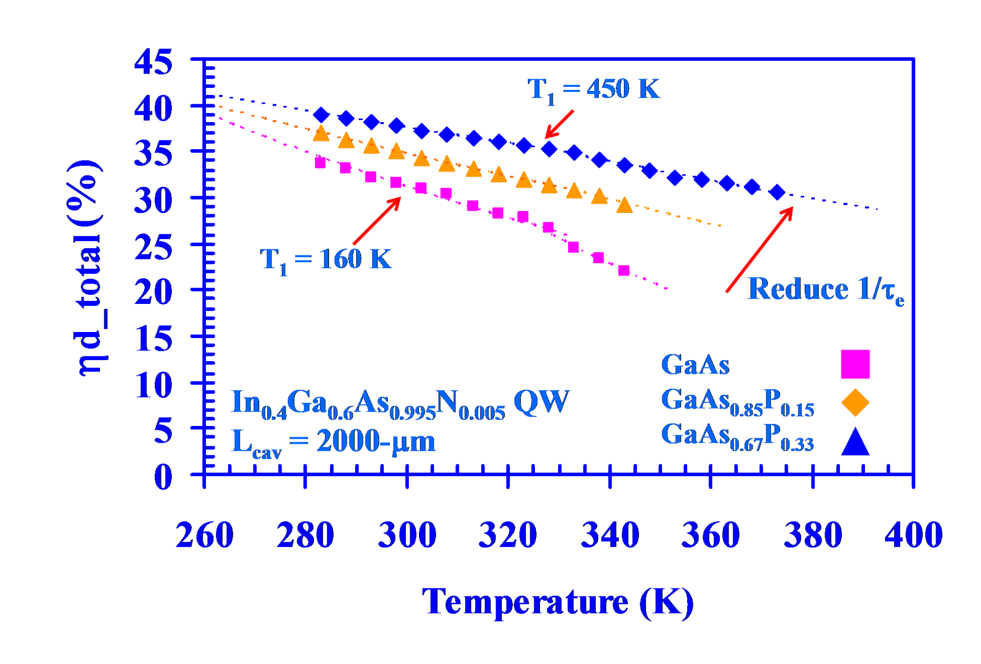
In our studies, we developed a detailed analysis of the below-threshold, at-threshold, and above-threshold current injection efficiency of single quantum well lasers, taking into account the recombination in the QW, recombination in the barriers (SCH), carrier transport and capture effect, and thermionic carrier escape effects. We find that the higher temperature sensitivity of the current injection efficiency for InGaAsN QW lasers can be understood from an increase in heavy-hole-leakage, due to the smaller hole-confinement in the InGaAsN QW lasers. By understanding the performance limitation of the InGaAsN QW lasers at high temperature, we are able to design structures with significantly increased hole confinement by surrounding the quantum well with GaAsP barriers. This improved structure of InGaAsN QW lasers with large bandgap GaAsP barriers allows suppression the thermionic hole leakage, resulting in very low threshold current density at elevated temperature. Utilizing GaAsP barriers in InGaAsN QW lasers also leads to the realization of InGaAsN QW lasers with temperature-insensitive slope efficiency at elevated temperature, confirming the predictions of our model. The improved threshold current density and external differential quantum efficiency for InGaAsN QW employing larger bandgap barriers of GaAsP were demonstrated, respectively.

Selected Relevant Publications:
- N. Tansu, J. Y. Yeh, and L. J. Mawst, “Experimental Evidence of Carrier Leakage in InGaAsN Quantum Well Lasers,” Appl. Phys. Lett., vol. 83(11), pp. 2112-2114, September 2003.
- N. Tansu, and L. J. Mawst, “Current Injection Efficiency of 1300-nm InGaAsN Quantum-Well Lasers,” J. Appl. Phys., vol. 97(5), Art. No. 054502, March 2005.
- J. Y. Yeh, L. J. Mawst, and N. Tansu, “The Role of Carrier Transport on the Current Injection Efficiency of InGaAsN Quantum-Well Lasers,” IEEE Photon. Technol. Lett., vol. 17(9), pp. 1779-1881, September 2005.
- (Invited Review Paper) N. Tansu, J. Y. Yeh, and L. J. Mawst, “Physics and Characteristics of 1200-nm InGaAs and 1300-1400 nm InGaAsN Quantum-Well Lasers by Metalorganic Chemical Vapor Deposition,” Journal of Physics: Condensed Matter Physics, vol. 16 (31), pp. S3277-S3318, August 2004.
- Physics of Optical Gain, Recombination Mechanisms, and Dynamics of Quantum Well Lasers
In addition to the pursuit of high performance InGaAsN QW lasers, we have also conducted further studies to better understand the physics of the InGaAsN QW gain media. Together with our collaborators, we have also performed various studies to understand the recombination mechanisms in the quantum well. The measurements include the optical gain measurements, true spontaneous emission measurements, and the high-frequency optical / electrical modulation of the QW gain media. These studies are conducted together with UW-Madison (Prof. L. J. Mawst), Cardiff University (Prof. P. Blood and Prof. P. M. Smowton), SUNY-Stony Brook (Prof. G. Belenky), Colorado State University (Prof. C. S. Menoni), and Marburg University / Sandia National Lab (Prof. S. W. Koch / Dr. Weng W. Chow). The studies are mainly conducted on the MOCVD-grown InGaAs QW and InGaAsN QW lasers on GaAs, emitting at 1200-nm and 1300-nm, respectively.
Several key results from our studies on highly-strained 1200-nm emitting InGaAs QW and 1300-nm InGaAsN QW lasers are:
a. Direct measurements of radiative efficiency and optical gain of InGaAs QW and InGaAsN QW active regions by using multi-segment measurement techniques. (with Cardiff University)
b. Carrier lifetime measurements and determinations of intrinsic frequency response from InGaAsN QW and InGaAsN QW gain media. (with Colorado State University)
c. Measurements of electron effective-mass of strain-compensated InGaAsN QW active region. (with Colorado State University)
d. Comparison of gain measurements and theoretical gain of InGaAsN QW gain media. (with State University of New York – Stony Brook, Marburg University – Germany, and Sandia National Laboratories)
e. Ultrafast carrier dynamic measurements of InGaAsN and InGaAs quantum wells. (with National Chiao-Tung University, Taiwan, Republic of China).
f. Direct measurements of carrier escape and capture in InGaAsN quantum wells lasers (with Colorado State University)
Selected Relevant Publications:
- D. J. Palmer, P. M. Smowton, P. Blood, J. Y. Yeh, L. J. Mawst, and N. Tansu, “Effect of Nitrogen on Gain and Efficiency in InGaAsN Quantum Well Lasers”, Appl. Phys. Lett., vol. 86 (7), Art. No. 071121, February 2005.
- O. Anton, D. Patel, C. S. Menoni, J. Y. Yeh, L. J. Mawst, J. M. Pikal, and N. Tansu, “Increased Monomolecular Recombination in MOCVD Grown 1.3-m InGaAsN–GaAsP–GaAs QW Lasers From Carrier Lifetime Measurements,” IEEE Photon. Technol. Lett., Vol 17 (5), 954-955, May 2005.
- A. Thranhardt, I. Kuznetsova, C. Schlichenmaier, S. W. Koch, L. Shterengas, G. Belenky, J. Y. Yeh, L. J. Mawst, N. Tansu, J. Hader, J. V. Moloney, and W. W. Chow, “Nitrogen Incorporation Effects on Gain Properties in GaInNAs Lasers: Experiment and Theory,” Appl. Phys. Lett. vol. 86, May 2005.
- L. Shterengas, G. Belenky, J. Y. Yeh, L. J. Mawst, and N. Tansu, “Differential Gain and Linewidth-Enhancement Factor in Dilute-Nitride GaAs-based 1.3m Diode Lasers,” IEEE J. Select. Topics. in Quantum Electron, vol. 11(5), pp. 1063-1068, September-October 2005.
- O. Anton, D. Patel, C. S. Menoni, J. Y. Yeh, T. T. Van Roy, L. J. Mawst, J. M. Pikal, and N. Tansu, “Frequency Response of Strain-Compensated InGaAsN/GaAsP/GaAs SQW Lasers,” IEEE J. Select. Topics. in Quantum Electron, vol. 11(5), pp. 1079-1088, September-October 2005.
- L. Xu, D. Patel, C. S. Menoni, J. Y. Yeh, L. J. Mawst, and N. Tansu, “Optical Determination of Electron Effective-Mass of Strain Compensated In0.4Ga0.6As0.995N0.005 / GaAs Single Quantum Well,” Appl. Phys. Lett., vol. 89, Art. 171112, October 2006.
- C. C. Hsu, J. H. Lin, Y. H. Lin, H. C. Kuo, S. C. Wang, W. F. Hsieh, N. Tansu, and L. J. Mawst, “Ultrafast Carrier Dynamics of InGaAsN and InGaAs Single Quantum Wells,” J. Phys. D: Appl. Phys., vol. 41(8), Art. 085107, April 2008.
- G. Tsvid, J. Kirch, L. J. Mawst, M. Kanskar, J. Cai, R. A. Arif, N. Tansu, P. M. Smowton, and P. Blood, “Spontaneous Radiative Efficiency and Gain Characteristics of Strained Layer InGaAs / GaAs Quantum Well Laser,” in IEEE J. Quantum Electron., vol. 44(8), pp. 732-739, August 2008.
- J. W. Ferguson, P. Blood, P. M. Smowton, H. Bae, T. Sarmiento, J. S. Harris, N. Tansu, and L. J. Mawst, “Optical Gain in GaInNAs and GaInNAsSb Quantum Wells,” IEEE J. Quantum Electron., vol. 47 (6), pp. 870-877, June 2011.
- L. F. Xu, D. Patel, C. S. Menoni, J. Y. Yeh, L. J. Mawst, and N. Tansu, “Experimental Evidence of the Impact of Nitrogen on Carrier Capture and Escape Times in InGaAsN / GaAs Single Quantum Well,” IEEE Photonics Journal (submitted).
- L. F. Xu, D. Patel, C. S. Menoni, J. M. Pikal, J. Y. Yeh, J. Y. T. Huang, L. J. Mawst, J. Zhang, and N. Tansu, “Carrier Recombination Dynamics Investigations of Strain Compensated InGaAsN Quantum Wells,” IEEE Photonics Journal (submitted).
- Interdiffused InGaAsP Quantum Dots Lasers on GaAs by Metal Organic Chemical Vapor Deposition
Self-assembled InGaAs quantum dot (QD) gain media grown by metal organic chemical vapor deposition (MOCVD) technique has a natural peak emission wavelength of around 1100-1200 nm due to its specific composition, shape, and size. In our works (in collaboration with Prof. L. J. Mawst at University of Wisconsin-Madison), a promising method to push emission wavelength of MOCVD-grown InGaAs QD gain media on GaAs to ~1000 nm by utilizing InGaAsP QD was demonstrated. The growths were conducted at Wisconsin, while all other experiments (rapid thermal annealing, fabrications, and characterizations) and simulations were conducted at Lehigh (by our PhD student). Incorporation of phosphorus species in the barrier layer into the QD is achieved by interdiffusion process. Our study consists of two main steps. Rapid thermal annealing (RTA) and low temperature photoluminescence (LT-PL) measurements are performed on MOCVD-grown InGaAs QD samples with GaAsP and GaAs barriers. All the samples are grown on GaAs substrate. In general, one observes an increasingly narrow full width at half max (FWHM) of PL spectrum with annealing time. For instance, after annealing for 300 s at 700ºC, sample with 20% P in the barrier and P-free barrier exhibit reduction in FWHM by 10.48 meV and 15.2 meV, respectively. The PL blueshift of sample annealed at 700ºC for 300 s with 20% P in the barrier is found to be 78 nm, while for P-free sample annealed under the same condition, the blueshift is observed to be only 64 nm. This marked difference in blueshifts is an indication of P-species incorporation into the QD, and this finding agrees well with the fact that P-containing QD possesses a larger energy gap that leads to shorter emission wavelength than P-free structure.
Diode laser devices based on unannealed and annealed QD gain media with 20% and 30% P in the barrier are fabricated. The annealed InGaAs/GaAs0.8P0.2 and InGaAs/GaAs0.7P0.3 QD laser devices exhibited reasonably low threshold current density of 202-288 A/cm2, with significant blue shift attributed to the outdiffusion of In from the QDs into the barrier region, and the diffusion of P from the GaAsP barrier into the InGaAs QD materials. One major potential application of this study includes EDFA pump lasers for optical telecommunication.
Selected Relevant Publications:
- R. A. Arif, N. H. Kim, L. J. Mawst, and N. Tansu, “Interdiffused InGaAsP Quantum Dots Lasers on GaAs by Metalorganic Chemical Vapor Deposition,” in Proc. of the MRS Fall Meeting 2005: Symposium EE: Progress in Semiconductor Materials V—Novel Materials and Electronic and Optoelectronic Applications, Boston, MA, USA, November-December 2005.
(ii) Dilute-Nitride Type-II InGaAsN-GaAsSb QW Lasers for 1550-nm and 3-4 micron
- Type-II GaAsSb-(In)GaAsN Quantum Well Lasers on GaAs
Though high-performance 1300-nm InGaAsN-QW lasers on GaAs have been realized, low-threshold 1550-nm InGaAsN QW lasers have yet to be realized. To extend the emission wavelength of the gain media for lasers on GaAs substrate into 1550-nm wavelength regime, we proposed a novel approach based on GaAsSb-(In)GaAsN type-II quantum well gain media on GaAs. In this structure, the electron-wells consist of (In)GaAsN layers and the hole-well consist of GaAsSb layer. This approach is an original and novel method to realize high-performance lasers emitting at wavelength of 1550-nm on a GaAs substrate. Strain-compensated structures with compressively-strained GaAsSb and tensile-strained GaAsN also allow the growth of multiple QW stages to achieve the necessary optical gain for lasers.
Material optical gain as a function of radiative current density at 300 K for optimized 1550-nm lasers based on GaAsSb-(In)GaAsN type-II QWs have been analyzed (collaboration of Naval Research Labs – Dr. Jerry Meyer and Dr. Igor Vurgaftman, University of Wisconsin-Madison, and Lehigh University). Energy dispersion, wavefunctions, and optical matrix elements were calculated using 10-band k∙p formalism, with band anti-crossing model employed to take into account the N-like band in the dilute-nitride layers. Our recent experimental work has also resulted in the first experimental realization of this novel dilute-nitride type-II QW gain media grown on GaAs substrate emitting with peak luminescence wavelength at 1600-nm. The envisioned GaAsSb-(In)GaAsN type-II QW edge-emitters and VCSELs are expected to be a competitive alternative approach to achieve a high-performance GaAs-based 1550-nm diode lasers.


Selected Relevant Publications:
- N. Tansu, and L. J. Mawst, “Design Analysis of 1550-nm GaAsSb-(In)GaAsN Type-II Quantum Well Laser Active Regions,” IEEE J. Quantum Electron., vol. 39(10), pp. 1205-1210, October 2003.
- I. Vurgaftman, J. R. Meyer, N. Tansu and L. J. Mawst, “(In)GaAsN-GaAsSb Type-II “W” Quantum-Well Lasers for Emission at =1.55 m,” in Appl. Phys. Lett., vol. 83(14), pp.2742-2744, Oct 2003.
- N. Tansu, L. J. Mawst, I. Vurgaftman, and J. Meyer, “GaAsSb-(In)GaAsN Type-II Quantum-Wells Lasers,” in Proc. of the 16th IEEE Laser and Electro-Optics Society (LEOS) Annual Meeting 2003, Tuczon, AZ, October-November 2003.
- (Invited Conference Paper) J. R. Meyer, I. Vurgaftman, N. Tansu, and L. J. Mawst, “Dilute-Nitride Type-II ‘W’ Quantum Well Lasers for the Near-IR and Mid-IR,” in Proc. of the SPIE Photonics West 2005, Novel In-Plane Semiconductor Lasers 2005, San Jose, CA, Jan 2005.
- J. Y. Yeh, A. A. Khandekar, B. E. Hawkins, T. F. Kuech, L. J. Mawst, J. R. Meyer, I. Vurgaftman, and N. Tansu, “Long Wavelength Emission from InGaAsN/GaAsSb Type-II ‘W’ Quantum Wells,” in Proc. of the 12th Biennial Workshop on Organometallic Vapor Phase Epitaxy (OMVPE) 2003, Big Sky Resort, Montana, July 2005.
- A. A. Khandekar, B. E. Hawkins, T. F. Kuech, J. Y. Yeh, L. J. Mawst, J. R. Meyer, and I. Vurgaftman, and N. Tansu, “Characteristics of GaAsN/GaAsSb type-II Quantum Wells on GaAs substrates grown by Metalorganic Chemical Vapor Deposition,” J. Appl. Phys. , vol. 98(12), Art. No. 123525, December 2005.
- J. Y. Yeh, L. J. Mawst, A. A. Khandekar, T. F. Kuech, J. R. Meyer, and I. Vurgaftman, and N. Tansu, “Long Wavelength Emission of InGaAsN/GaAsSb Type-II “W” Quantum Wells,” Appl. Phys. Lett., vol. 88(5), Art. No. 051115, January 2006.
- (Invited Journal Paper) L. J. Mawst, J. Y. T. Huang, D. P. Xu, J. Y. Yeh, and G. Tsvid, T. F. Kuech, and N. Tansu, “MOCVD grown Dilute-Nitride Type-II Quantum Wells,” IEEE Selected Topics in J. Quantum Electron., vol. 14(4), pp. 979-991, July / August 2008.
Relevant US Patents:
- Nelson Tansu, and Luke J. Mawst, “Type-II Quantum Well Optoelectronics Devices,” Novel techniques to achieve 1500-3000 nm wavelength emission on GaAs”, US Patent No. 6,791,104; approved on September 14th 2004.
- Dilute-Nitride Type-II “W” Quantum Well Lasers on InP
In collaboration with Naval Research Lab (Dr. J. R. Meyer and Dr. I. Vurgaftman) and the UW-Madison (Prof. L. J. Mawst), we have also proposed to extend the technology of dilute-nitride type-II “W” quantum well gain media for 3-5 μm mid-infrared laser application on InP substrate. Previously, the interband lasers to achieve mid-infrared range (3-5 μm) can only be achievable utilizing the quantum well structure grown on GaSb substrate. The original and novel approach is to utilize the GaAsSb-InGaAsN type-II quantum well gain media grown on InP, which should allow the realization of mid-infrared (3-5 m) lasers on the more-conventional InP substrate. This work potentially should allow the realization of mid-infrared interband semiconductor lasers on conventional substrate capable of operating at room-temperature under continuous-wave operation.

Selected Relevant Publications:
- I. Vurgaftman, J. R. Meyer, L. J. Mawst, and N. Tansu, “Dilute-Nitride Mid-Infrared Type-II ‘W’ Quantum-Well Lasers on InP Substrates”, in Proc. of the IEEE/OSA Conference on Lasers and Electro-Optics (CLEO) 2004, San Francisco, CA, May 2004.
- I. Vurgaftman, J. R. Meyer, N. Tansu, and L. J. Mawst, “InP-Based Dilute-Nitride Mid-Infrared Type-II “W” Quantum-Well Lasers,” J. Appl. Phys., vol. 96(8), pp. 4653-4655, October 2004.
- (Invited Conference Paper) J. R. Meyer, I. Vurgaftman, N. Tansu, and L. J. Mawst, “Dilute-Nitride Type-II ‘W’ Quantum Well Lasers for the Near-IR and Mid-IR,” in Proc. of the SPIE Photonics West 2005, Novel In-Plane Semiconductor Lasers 2005, San Jose, CA, Jan 2005.
Relevant US Patents:
- Luke J. Mawst, Nelson Tansu, Igor Vurgaftmann, and Jerry R. Meyer, “Type-II Quantum Well Mid-Infrared Optoelectronic Devices“ Novel techniques to achieve 3000-5000 nm wavelength emission. Lasers, US Patent No. 7,256,417; approved on August 14th 2007.
(iii) V.3. Interdiffused InGaAsSbN Quantum Well Lasers for 1300-1550 nm Regimes
- Interdiffused InGaAsSbN Quantum Well for 1300-1550 nm Lasers
InGaAsSbN QW grown by molecular beam epitaxy (MBE) is a very promising approach to realize type-I quantum well on GaAs substrate for achieving diode lasers emitting at 1550-nm, with very promising results produced by Prof. Jim Harris’ group at Stanford. Nonetheless, the pursuit of InGaAsSbN material systems growth by MOCVD is still immature, due to the challenges in incorporating both Sb- and dilute-N-species into InGaAs material systems simultaneously under optimum MOCVD growth conditions.

Selected Relevant Publications:
- R. A. Arif, and N. Tansu, “Interdiffused InGaAsSbN Quantum Wells on GaAs for 1300-1550 nm Lasers,” in Proc. of the SPIE Photonics West 2005, Physics and Simulation of Optoelectronics Devices XIII, San Jose, CA, Jan 2005.
- R. A. Arif, and N. Tansu, “Interdiffused SbN-Based Quantum Wells on GaAs for 1300-1550 nm Lasers: Theory and Experiments,” in IEEE Semiconductor Lasers Workshop 2005, Baltimore, MD, May 2005.
- R. A. Arif, and N. Tansu, “Interdiffused SbN-Based Quantum Wells on GaAs for 1300-1550 nm Lasers,” in Proc. of the MRS Fall Meeting 2005: Symposium EE: Progress in Semiconductor Materials V—Novel Materials and Electronic and Optoelectronic Applications, Boston, MA, USA, November-December 2005.
- (Invited Book Chapter) Ronald A. Arif, and Nelson Tansu, ”Interdiffused InGaAsSbN Quantum Well for 1300-1550 Diode Lasers on GaAs,” Book Chapter in “Dilute-Nitrides: Physics and Applications” (Edited by: Dr. Ayse Erol), Springer Verlag, January 2008.
(iv) High Efficiency III-Nitride Light Emitting Diodes for Solid State Lighting
“Physics, Devices, and MOCVD Epitaxy of III-Nitride Semiconductor Nanostructures for High-Efficiency Solid State Lightings”
Our research efforts have focused on physics, MOCVD epitaxy, and device physics of III-Nitride semiconductor optoelectronics and nanostructures. Among the most important applications addressed in our research is the field of solid state lighting. Other applications of III-Nitride semiconductors include development of InN-based materials by MOCVD for photovoltaic and Terahertz optoelectronics, and InGaN-based thermoelectric materials.
One of the largest uses of energy in United States is electrical power for lighting, which accounts for approximately 21 % of the US’s total electrical energy use. High-efficiency visible solid state emitters for lighting lead to efficient use of energy, which in turn will lead to significant cost savings in energy consumption for the nation. Currently group III-Nitride semiconductor based light emitting diodes (LEDs) have shown tremendous promise in signage and display applications, and the III-Nitride semiconductor materials have shown tremendous potential as candidates for high-efficiency white-light solid state lightings. It is estimated that the use of white light solid state LEDs for illumination will reduce energy consumption in the U.S. by ~150-200 billion kilowatts-hours (kWh) annually, which translate to saving of ~$15-25 billion / annum. In addition to the positive economic impact of high-efficiency LEDs, more efficient use of electrical energy also reduces the negative environmental impact of generating electrical energy by conventional means. High-efficiency solid-state lighting as a low-cost lighting solution will also have an impact in developing countries, where electricity and illumination are scarce.
Our research program focused on integrated research and educational programs on approaches for achieving high-efficiency group III-Nitride semiconductor light emitting diodes for solid state lighting. In particular, the proposed research will focus on low-cost and practical approaches for addressing challenges in achieving:
1) Improvement of radiative efficiency and optical gain of InGaN-based quantum wells by using novel InGaN-based quantum wells / dots with improved matrix element design
2) Improvement of light extraction efficiency of III-Nitride LEDs by using low-cost and practical approach of SiO2 / polystyrene microlens arrays
3) Nano-heteroepitaxy of low-dislocation density GaN based materials on patterned AGOG sapphire substrates
4) Employing surface plasmon coupled InGaN quantum wells light emitting diodes
5) Employing novel quantum well – barrier design for suppressing efficiency-droop in InGaN quantum wells light-emitting diodes
6) Novel approaches for monolithic electrically-injected white light-emitting diodes for solid state lighting
All aspects (design, growth, device physics, and device fabrications) of these research programs are conducted by PhD students and postdoctoral researchers in our research group at Lehigh University.
- Novel III-Nitride Quantum Wells / Dots Structures + Surface Plasmon LEDs / Lasers (Internal Quantum Efficiency, Green Gap, Efficiency-Droop and Optical Gain)
In these works, we investigated novel InGaN-based QW structures for improved active media for III-Nitride LEDs and lasers emitting in the blue up to green spectral regimes (and beyond). One of the main chalenges related to conventional nitride-based InGaN QW is the reduced electron-to-photon conversion efficiency (radiative efficiency), in particular as the emission wavelength is extended into the green and yellow / red emission regimes. The physical reason is related to the large inherent built-in electric field (spontaneous and piezoelectric polarization field) inside the QW layer, which results in the “charge separation” effect (quantum-mechanical spatial distributions of electron and hole to be separated from one another). The separation of electron and hole spatial distribution in the QW leads to reduced radiative recombination rate and efficiency of the conventional light emitting diodes (LEDs). Our research group at Lehigh investigated several novel active regions for suppressing the “charge separation” in the III-Nitride QW, by designing the InGaN-based quantum well with improved optical matrix elements (and overlap |e-hh|2) using the following structures:
a. Staggered / Graded InGaN Type-I Quantum Wells
b. Nitride Type-II “W” Quantum Wells (using type-II InGaN-GaNAs QW)
c. Strain-Compensated InGaN-GaNAs Quantum Wells
In addition, our research groups have also focused on the use of surface Plasmon LEDs by using double metallic configuration, ultra-high density quantum dots, growth of GaN on Si substrate, new active region and substrate technologies, and novel QW-barrier design for achieving high internal quantum efficiency in nitride LEDs. The goal of these works is to achieve high internal quantum efficiency (and optical gain) for nitride-based LEDs (and lasers) and suppression of efficiency-droop in nitride LEDs.
Selected Relevant Publications (for complete publications, please refer to CV):
Staggered InGaN Quantum Wells
- R. A. Arif, Y. K. Ee, and N. Tansu, “Polarization Engineering via Staggered InGaN Quantum Wells for Radiative Efficiency Enhancement of Light Emitting Diodes,” Appl. Phys. Lett., vol. 91 (9), Art. 091110, August 2007. [Also featured in the Virtual Journal of Nanoscale Science and Technology; and Laser Focus World – News Break section, Nov 2007]
- (Invited Journal Paper) R. A. Arif, Y. K. Ee, and N. Tansu, “Nanostructure Engineering of InGaN-Based Active Regions for Improved III-Nitride Gain Media Emitting at 420-550 nm,” in Physica Stat. Solidi A, vol. 205 (1), pp. 96-100, January 2008.
- R. A. Arif, H. Zhao, Y. K. Ee, and N. Tansu, “Spontaneous Emission and Characteristics of Staggered InGaN Quantum Wells Light Emitting Diodes,” IEEE J. Quantum Electron., vol. 44(5-6), pp.573-580, May-June 2008.
- H. P. Zhao, R. A. Arif, and N. Tansu, “Design Analysis of Staggered InGaN Quantum Wells Light-Emitting Diodes at 500-540 nm,” IEEE J. Sel. Top. Quantum Electron., vol. 15 (4), pp. 1104-1114, July-August 2009.
- H. P. Zhao, G. S. Huang, G. Y. Liu, X. H. Li, J. D. Poplawsky, S. Tafon Penn, V. Dierolf, and N. Tansu, “Growths of Staggered InGaN Quantum Wells Light-Emitting Diodes Emitting at 520-525 nm Employing Graded Growth-Temperature Profile,” Appl. Phys. Lett., vol. 95(6), Art. 061104, August 2009. [Top 20 Most Downloaded Articles in Applied Physics Letters, Aug 2009]
- (Invited Journal Paper) H. P. Zhao, G. Y. Liu, X. H. Li, R. A. Arif, G. S. Huang, J. D. Poplawsky, S. Tafon Penn, V. Dierolf, and N. Tansu, “Design and Characteristics of Staggered InGaN Quantum Well Light-Emitting Diodes in the Green Spectral Regimes,” IET Optoelectronics, vol. 3(6), pp. 283-295, December 2009.
- (Invited Review Article) N. Tansu, H. P. Zhao, G. Y. Liu, X. H. Li, J. Zhang, H. Tong, and Y. K. Ee, “Breakthrough in Photonics 2009: III-Photonics”, IEEE Photonics Journal, vol. 2 (2), pp. 241-248, April 2010.
- H. P. Zhao, and N. Tansu, “Optical Gain Characteristics of Staggered InGaN Quantum Well Lasers,” J. Appl. Phys., vol. 107, Art. 113110, June 2010.
- H. P. Zhao, G. Y. Liu, and N. Tansu, “Analysis of InGaN-Delta-InN Quantum Wells for Light-Emitting Diodes,” Appl. Phys. Lett., vol. 97, Art. 131114, September 2010.
- (Invited Journal Paper) H. P. Zhao, G. Y. Liu, J. Zhang, J. D. Poplawsky, V. Dierolf, and N. Tansu, “Approaches for High Internal Quantum Efficiency Green InGaN Light-Emitting Diodes with Large Overlap Quantum Wells,” Optics Express, vol. 19 (S4), pp. A991-A1007, July 2011.
- G. Sun, G. B. Xu, Y. J. Ding, H. P. Zhao, G. Y. Liu, J. Zhang, and N. Tansu, “Investigation of Fast and Slow Decays in InGaN/GaN Quantum Wells,” Appl. Phys. Lett., vol. 99, Art. 081104, Aug 2011.
Type-II InGaN-GaNAs Quantum Wells - R. A. Arif, H. Zhao, and N. Tansu, “Type-II InGaN-GaNAs Quantum Wells Active Regions for Lasers Applications,” Appl. Phys. Lett. vol. 92(1), Art. No. 011104, January 2008.
- H. P. Zhao, R. A. Arif, and N. Tansu, “Self Consistent Gain Analysis of Type-II ‘W’ InGaN-GaNAs Quantum Well Lasers,” J. Appl. Phys., vol. 104 (4), Art. 043104, August 2008.
Strain-Compensated InGaN-AlGaN Quantum Wells - H. Zhao, R. A. Arif, Y. K. Ee, and N. Tansu, “Optical Gain Analysis of Strain-Compensated InGaN–AlGaN Quantum Well Active Regions for Lasers Emitting at 420-500 nm,” Optical and Quantum Electronics, vol. 40 (1), January 2008.
- H. P. Zhao, R. A. Arif, Y. K. Ee, and N. Tansu, “Self-Consistent Analysis of Strain-Compensated InGaN-AlGaN Quantum Wells for Lasers and Light Emitting Diodes,” IEEE J. Quantum Electron., vol. 45(1-2), pp. 66-78, January-February 2009.
Selective Area Epitaxy of Ultrahigh Density InGaN Quantum Dots LEDs - G. Y. Liu, H. P. Zhao, J. Zhang, J. H. Park, L. J. Mawst, and N. Tansu, “Selective Area Epitaxy of Ultra-High Density InGaN Quantum Dots by Diblock Copolymer,” Nanoscale Res. Lett., vol. 6, Art. 342, April 2011.
InGaN Quantum Wells LEDs on Ternary Substrates - J. Zhang, and N. Tansu, “Improvement in Spontaneous Emission Rates for InGaN Quantum Wells on Ternary InGaN Substrate for Light-Emitting Diodes,” J. Appl. Phys., vol. 110 (11), Art. 113110, December 2011.
Surface Plasmon Coupled InGaN Quantum Wells LEDs for High Internal Quantum Efficiency - H. P. Zhao, J. Zhang, G. Y. Liu, and N. Tansu, “Surface Plasmon Dispersion Engineering via Double-Metallic Au / Ag Layers for III-Nitride Based Light-Emitting Diodes,” Appl. Phys. Lett., vol. 98, Art. 151115, April 2011.
Self-Assembled InGaN Quantum Dots - Y. K. Ee, H. Zhao, R. A. Arif, M. Jamil, and N. Tansu, “Self-Assembled InGaN Quantum Dots on GaN Grown by Metalorganic Vapor Phase Epitaxy ,” J. Crystal Growth, vol. 310 (7-9), pp. 2320-2325, April 2008.
- Y. K. Ee, R. A. Arif, M. Jamil, and N. Tansu, “MOCVD Epitaxy and Optical Properties of Self-Assembled InGaN Quantum Dots via Stranski-Kastranow Growth Mode Emitting at 520-nm,” in Proc. of the IEEE/OSA Conference on Lasers and Electro-Optics (CLEO) 2007, paper CME3, Baltimore, MD, May 2007.
- Y. K. Ee, H. Zhao, R. A. Arif, M. Jamil, and N. Tansu, “Self-Assembled InGaN Quantum Dots on GaN Grown by Metalorganic Vapor Phase Epitaxy ,” in Proc. of the 13th Biennial Workshop on Organometallic Vapor Phase Epitaxy (OMVPE) 2007, Salt Lake City, UT, August 2007.
Novel Quantum Wells – Barrier Structures for Efficiency Droop Suppression - H. P. Zhao, G. Y. Liu, R. A. Arif, and N. Tansu, “Current Injection Efficiency Quenching Leading to Efficiency Droop in InGaN Quantum Well Light-Emitting Diodes,” Solid-State Electronics, vol. 54(10), pp. 1119–1124, October 2010 Growth of Crack-Free GaN on Silicon Substrates
- M. Jamil, R. A. Arif, Y. K. Ee, H. Tong, J. B. Higgins, and N. Tansu, “MOCVD Epitaxy of InN Films on GaN Templates Grown on Sapphire and Silicon (111) Substrates,” in Physica Stat. Solidi (a), vol. 205 (7), pp. 1619-1624, July 2008.
- Novel Approach for Enhancement of Light Extraction Efficiency of III-Nitride LEDs by Using SiO2 / Polystyrene Microlens Arrays = Colloidal Lithography Approach
The total internal reflection on the GaN / air interface results in narrow escape cone probability of only ~4 % from top surface of the nitride-based LEDs device. Several approaches (ie. photonic crystal, nano-pyramid, die-shaping, roughening, and graded-index matched layer) had been proposed with their respective advantages and limitations, but primarily the high cost (with the use of e-beam lithography, or die shaping) and low yield (ie. roughening) are the two main limitations of the existing approaches.
In our research group at Lehigh (collaboration of Tansu’s group and Gilchrist’s group at Lehigh), we pursue a novel approach to improve the light extraction efficiency of InGaN quantum wells light emitting diodes (LEDs) using SiO2 / polystyrene microlens arrays. The depositions of microlens arrays were achieved by employing low-cost and practical approach of rapid convective deposition method, and this approach leads to formation of 2-D hexagonal close-packed SiO2 / polystyrene microlens arrays on the p-GaN contact layer [as shown in figure 10(a)]. The implementation of these microlens arrays on InGaN QW LEDs has led to significant improvement up to a +200% increase of the LEDs output power [shown in figure 10(b)], which is in good agreement with predicted theory. This approach also leads to a low-cost and straight-forward solution to induce controlled surface roughness on top of the LEDs for improving light extraction efficiency, without using the costly e-beam lithography process. In addition, we have also developed method to achieve concave microstructure LEDs and LEDs employing microlens arrays with various aspect ratios for engineering the far-field radiation patterns.
Selected Relevant Journal Publications:
- Y. K. Ee, R. A. Arif, N. Tansu, P. Kumnorkaew, and J. F. Gilchrist, “Enhancement of Light Extraction Efficiency of InGaN Quantum Wells Light Emitting Diodes Using SiO2 / Polystyrene Microlens Arrays,” Appl. Phys. Lett., vol. 91(22), Art. No. 221107, November 2007. [Also featured in the Laser Focus World, Jan 2008]
- (Cover Article) P. Kumnorkaew, Y. K. Ee, N. Tansu, and J. F. Gilchrist, “Deposition of Microsphere Monolayers for Fabrication of Microlens Arrays,” Langmuir, vol. 24 (21), pp. 12150-12157, November 2008.
- Y. K. Ee, P. Kumnorkaew, R. A. Arif, H. Tong, H. P. Zhao, J. F. Gilchrist, and N. Tansu, “Optimization of Light Extraction Efficiency of III-Nitride Light Emitting Diodes with Self-Assembled Colloidal-based Microlenses,” IEEE J. Sel. Top. Quantum Electron., vol. 15 (4), pp. 1218-1225, July-August 2009.
- Y. K. Ee, P. Kumnorkaew, R. A. Arif, H. Tong, J. F. Gilchrist, and N. Tansu, “Light Extraction Efficiency Enhancement of InGaN Quantum Wells Light-Emitting Diodes with Polydimethylsiloxane Concave Microstructures,” Optics Express, vol. 17 (16), pp. 13747-13757, August 2009. [Also featured in the Laser Focus World, August 2009]
- X. H. Li, R. B. Song, Y. K. Ee, P. Kumnorkaew, J. F. Gilchrist, and N. Tansu, “Light Extraction Efficiency and Radiation Patterns of III-Nitride Light-Emitting Diodes with Colloidal Microlens Arrays with Various Aspect Ratios,” IEEE Photonics Journal, vol. 3 (3), pp. 489-499, June 2011.
- W. H. Koo, W. Youn, R. B. Song, X. H. Li, L. Zhao, P. F. Zhu, N. Tansu, and F. So, “Light extraction of organic light emitting diodes using defective hexagonal-close-packed array,” Advanced Functional Materials, (submitted).
- Nanoheteropitaxy Approach for Low Dislocation Density GaN Semiconductors on Nano-Patterned Sapphire Substrate
The existence of large lattice mismatch between GaN semiconductor and sapphire substrates leads to the formation of high misfit strain and threading dislocation density in the grown semiconductors. The high density of threading dislocations has been linked to failure of lasers and breakdown of p-n junctions. Hence, for high performance and reliable nitride-based LEDs and laser diodes, threading dislocation density has to be reduced. Several approaches had been implemented to reduce the threading dislocation density in GaN epitaxial layers, such as lateral epitaxial overgrowth (LEO), pendeo epitaxy, and cantilever epitaxy. These approaches have demonstrated reduced dislocation densities in the GaN layers in the range of 106 – 107 cm-2, but the low-defect regions are only limited to 5-10 µm wide stripe ridges. Recently, Prof. S. D. Hersee’s group (University of New Mexico) proposed proposed a technique based on nanoheteroepitaxy (NHE) of GaN on nano-patterned silicon and sapphire substrates, which uses a nano-pillar growth mode for reducing the dislocation density of the GaN film. The advantage of NHE process on nano-patterned sapphire substrate is the possibility of achieving low defect density GaN materials in large-area regimes (ie. entire wafer).
Our research group, in collaboration with Prof. Helen M. Chan and Prof. R. P. Vinci (Material Science Engineering, Lehigh), has investigated the nanoheteroepitaxy of GaN semiconductors on nanopatterned sapphire substrates. In our approach, instead of patterning the sapphire substrate via an etching technique, we employ a novel AGOG process that enables creation of single crystal Al2O3 islands on the sapphire substrates. ‘AGOG’ is an acronym for the unique process of creating these nanostructures via oxidation of deposited aluminum (Al) islands to form Al2O3 and subsequently annealing to convert the islands to single crystal (note: the AGOG process was originally developed by Prof. Chan’s group at Lehigh). The nanoheteroepitaxy of III-Nitride semiconductor is conducted using metalorganic chemical vapor deposition (MOCVD) process. Promising preliminary results have indicated an order of magnitude defect density reduction, and 2-times improvement in the photoluminescence intensity of InGaN QW grown on GaN template on patterned AGOG sapphires.
Selected Relevant Publications:
- Y. K. Ee, J. M. Biser, W. Cao, H. M. Chan, R. P. Vinci, and N. Tansu, “Metalorganic Vapor Phase Epitaxy of III-Nitride Light-Emitting Diodes on Nano-Patterned AGOG Sapphire Substrate by Abbreviated Growth Mode,” IEEE J. Sel. Top. Quantum Electron., vol. 15 (4), pp. 1066-1072, July-August 2009.
- Y. K. Ee, X. H. Li, J. E. Biser, W. Cao, H. M. Chan, R. P. Vinci, and N. Tansu, “Abbreviated MOVPE Nucleation of III-Nitride Light-Emitting Diodes on Nano-Patterned Sapphire,” J. Crys. Growth, vol. 312 (8), pp. 1311-1315, April 2010.
- W. Cao, J. M. Biser, Y. K. Ee, X. H. Li, N. Tansu, R. P. Vinci, and H. M. Chan, “Dislocation Structure of GaN Films Grown on Planar and Nano-Patterned Sapphire,” J. Appl. Phys., vol. 110, Art. 053505, September 2011.
(v) MOCVD Epitaxy of InN Semiconductors for Solar Cells and Terahertz Photonics
Recently, it has been discovered that the bandgap of InN was at about ~0.65-0.7 eV. The small bandgap of InN materials corresponds to long absorption cut off wavelength at ~1850 nm, which is applicable for covering the solar spectrum up to ~1850 nm regime. In particular, the availability of high-quality InN materials allows the additional coverage of solar spectrum in the ~1400-1850 nm regimes. Tandem solar cells can be implemented in the III-Nitride semiconductor material systems, to realize nitride-based monolithic high-efficiency solar cells with full spectrum utilization. As GaN has an energy bandgap of 3.4 eV, the solar spectrum from 280-nm up to 360-nm can be covered by the GaN-based solar cell. By engineering the InGaN alloys from low In-content (~33%) InGaN up to InN alloy, the solar spectrum from deep UV regime (~280-nm) up to ~1800-nm can be covered by varying the In-composition in the multiple junction cell. The ability of InGaN alloy in covering almost all the solar spectrum makes this alloy (InxGa1-xN) an excellent material candidate for making full spectrum high-efficiency solar cells. In addition to solar cells applications, the InN compound has also attracted great attention in particular for its potential efficient generation of terahertz radiation.
In contrast to the more mature development of MBE (molecular beam epitaxy)-grown InN, the growths of InN by metalorganic chemical vapor deposition (MOCVD) have resulted in promising results only recently. The growths of high-quality single crystalline InN films by MOCVD are still challenging. Different methods have been developed to grow InN films, and the quality of InN films has significantly improved. Commonly, high V/III ratios of input precursors are employed to achieve the droplet-free InN films. In order to increase the growth rate as well as to avoid large consumption of group V source, efforts have been made, and growths under comparatively low V/III ratios have also been reported. However, the droplet-free growth of InN under low V/III ratios is not common to all MOCVD reactor geometries.
In our research works, we developed pulsed MOCVD technique to grow narrow band gap (0.77 eV) InN without the requirement of high V/III ratios of input precursors [shown in figures 11(a) and 11(b)]. The use of pulsed-MOCVD growth resulted in droplet-free narrow-bandgap InN films grown on GaN/sapphire substrates. In pulsed-growth, NH3 was constantly flown into the reactor with pulsing of the TMIn source during the InN growth. In the pulsing of group-III precursor, TMIn was sent into the reactor chamber for a 30-second pulse and followed by an 18-second pause (no TMIn) with total period of 48 seconds for each cycle. The use of this pulsed growth mode allow the growth of high-quality narrow bandgap (0.77 eV) InN semiconductor with narrow XRD FWHM and reasonably-high electron mobility [e = 681 cm2/(V.sec)]. The growth optimizations are still conducted for reducing the background doping concentration, and improving surface morphology.
Recently, our group has collaborated with Prof. Yujie Ding’s group at Lehigh to conduct studies of terahertz generation from InN thin film and InGaN / GaN multiple QWs by using ultrafast laser experiments. The studies have shown very promising results from both the QW and thin film studies. The mechanisms behind the generation of terahertz radiation from MOCVD-grown InN thin film (via resonant optical rectification) is shown as different than the mechanism of terahertz radiation generation from the InGaN / GaN multiple QWs (via screening built-in field by photogenerated carriers). The preliminary results have shown the terahertz generation from the pulsed-MOCVD grown InN samples, as comparable to the results reported by MBE technique. Recently, we have also extended the works for THz generation from the InGaN / GaN quantum wells samples.
Selected Relevant Publications:
- M. Jamil, R. A. Arif, Y. K. Ee, H. Tong, J. B. Higgins, and N. Tansu, “MOCVD Epitaxy of InN Films on GaN Templates Grown on Sapphire and Silicon (111) Substrates,” in Physica Stat. Solidi (a), vol. 205 (7), pp. 1619-1624, July 2008.
- M. Jamil, H. P. Zhao, J. Higgins, and N. Tansu, “Influence of Growth Temperature and V/III Ratio on the Optical Characteristics of Narrow-Band Gap (0.77 eV) InN Grown on GaN / Sapphire Using Pulsed MOVPE,” in J. Crys. Growth, vol. 310(23), pp. 4947-4953, November 2008.
- M. Jamil, H. P. Zhao, J. Higgins, and N. Tansu, “MOVPE and Photoluminescence of Narrow Band Gap (0.77 eV) InN on GaN / Sapphire by Pulsed Growth Mode,” in Physica Stat. Solidi (a), vol. 205(12), pp. 2886-2891, December 2008.
- G. Xu, Y. J. Ding, H. P. Zhao, M. Jamil, G. Y. Liu, N. Tansu, I. B. Zotova, C. E. Stutz, D. E. Diggs, N. Fernelius, F. K. Hopkins, C. S. Gallinat, G. Koblmüller, and J. S. Speck, “THz Generation from InN Films due to Destructive Interference between Optical Rectification and Photocurrent Surge,” Semiconductor Science and Technology, vol. 25 (1), Art. 015004, January 2010.
- G. Sun, G. Xu, Y. J. Ding, H. P. Zhao, G. Y. Liu, J. Zhang, and N. Tansu, “Efficient Terahertz Generation from Multiple InGaN / GaN Quantum Wells,” IEEE J. Sel. Top. Quantum Electron., vol. 17(1), pp. 48-53, January-February 2011.
- E. Readinger, G. Chern, H. Shen, M. Wraback, R. A. Arif, Y. K. Ee, and N. Tansu, “Optical and Physical Properties of In-faced InN/InGaN Multi-Quantum Wells Grown on GaN Templates by Plasma-Assisted Molecular Beam Epitaxy,” in Proc. of the North America Molecular Beam Epitaxy (NAMBE) Conference 2007, Alburqueque, NM, September 2007.
(vi) III-Nitride Thermoelectric Materials and Devices
Recently, thermoelectric materials draw a lot of attention due to their applications for optoelectronics device cooling and heat recycling for electric power generation. InGaN-based materials have recently been demonstrated to have promising thermoelectric properties with potential applications for nitride-based laser devices cooling and thermoelectric power generators.
In this work, we analyzed theoretically the thermoelectric properties of n-type wurtzite InGaN semiconductors. The electronic transports in InGaN alloys were analyzed using Boltzmann transport equation considering the dominant mechanisms of energy-dependent electron scatterings. The total average relaxation rate includes contributions from the charged dislocation scattering, ionized impurity scattering, polar optical-phonon scattering, deformation potential acoustic phonon scattering, and piezoelectric acoustic phonon scattering. The thermoelectric properties of both InN and InGaN alloys were then carried out for thermal conductivity, electrical conductivity, and the Seebeck coefficient, and figure of merits (Z*T). Comprehensive model on lattice thermal conductivity is required for accurate modeling of the thermoelectric properties. At room temperature, the Seebeck coefficient ranges from -4×10⁻⁴ V/K up to -1×10⁻⁴ V/K for InGaN alloy for doping level ranging from 1017 cm-3 to 1019 cm-3, which are in good agreement with experimental results. For a particular doping level, the Seebeck coefficient for InGaN alloy decreases as temperature increases. The figures of merits (Z*T) for optimized InGaN alloy are computed as high as 0.1-0.2 for temperature range of 300-500 K, in agreement with the reported experimental results. The improved thermoelectric properties of InGaN can be attributed to the increased electrical conductivity and the reduced lattice thermal conductivity.
In addition, we have also investigated the thermoelectric characteristics of AlInN materials grown by MOCVD. The investigation of this new material have resulted in record Z*T values (~0.532) at room temperature, in comparison with other semiconductor technologies. The discovery of the large Z*T values in AlInN has also led to further investigation and recent funding (by NSF) to work on pushing this material systems for integration in nitride-based high power transistor, LEDs, and lasers devices.
Selected Relevant Publications:
- H. Tong, J. Zhang, G. Y. Liu, J. Herbsommer, G. S. Huang, and N. Tansu, “Thermoelectric Properties of Lattice-Matched AlInN Alloy Grown by Metalorganic Chemical Vapor Deposition,” Appl. Phys. Lett., vol. 97, Art. 112105, September 2010.
- J. Zhang, H. Tong, G. Y. Liu, J. A. Herbsommer, G. S. Huang, and N. Tansu, “Characterizations of Seebeck Coefficients and Thermoelectric Figures of Merit for AlInN Alloys with Various In-Contents,” J. Appl. Phys., vol. 109(5), Art. 053706, March 2011.
- J. Zhang, S. Kutlu, G.Y.Liu, and N. Tansu, “High-Temperature Characteristics of Seebeck Coefficients for AlInN Alloys Grown by Metalorganic Vapor Phase Epitaxy,” J. Appl. Phys., vol. 110, Art. 043710, August 2011.
- G. Y. Liu, J. Zhang, X. H. Li, G. S. Huang, T. Paskova, K. R. Evans, H. P. Zhao, and N. Tansu, “Metalorganic Vapor Phase Epitaxy and Characterizations of Nearly-Lattice-Matched AlInN Alloys on GaN / Sapphire Templates and Free-Standing GaN Substrates,” J. Crys. Growth, vol. 340 (1), pp. 66-73, February 2012.
(vii) Physics of III-Nitride Based Deep UV Gain Media
The use of AlGaN and AlInN alloys enable the pursuit of deep UV optoelectronics. The availability of deep UV lasers and LEDs will enable various applications in water purification, free space communication, and biochemical detection. Recently, our group has started theoretical and experimental investigation of AlGaN and AlInN based deep UV quantum wells. Several of the key works have been published in identify the limitation of the conventional AlGaN QW in accessing the deep UV and mid UV spectral regime, and our subsequent works have also pointed out the possible structures to address the low gain in the AlGaN QW in the mid UV spectral regime.
Selected Relevant Publications:
- J. Zhang, H. P. Zhao, and N. Tansu, “Effect of Crystal-Field Split-Off Hole and Heavy-Hole Bands Crossover on Gain Characteristics of High Al-Content AlGaN Quantum Well Lasers,” Appl. Phys. Lett. vol. 97, Art. 111105, September 2010.
- J. Zhang, H. P. Zhao, and N. Tansu, “Large Optical Gain AlGaN-Delta-GaN Quantum Wells Laser Active Regions in Mid- and Deep-Ultraviolet Spectral Regimes,” Appl. Phys. Lett., vol. 98, Art. 171111, April 2011.
- G. Sun, Y. J. Ding, G. Y. Liu, G. S. Huang, H. P. Zhao, N. Tansu, and J. B. Khurgin, “Photoluminescence Emission in Deep Ultraviolet Region from GaN/AlN Asymmetric-Coupled Quantum Wells,” Appl. Phys. Lett., vol. 97, Art. 021904, July 2010.
- G. Y. Liu, J. Zhang, X. H. Li, G. S. Huang, T. Paskova, K. R. Evans, H. P. Zhao, and N. Tansu, “Metalorganic Vapor Phase Epitaxy and Characterizations of Nearly-Lattice-Matched AlInN Alloys on GaN / Sapphire Templates and Free-Standing GaN Substrates,” J. Crys. Growth, vol. 340 (1), pp. 66-73, February 2012.
(viii) Computational Nanostructures + Computational Photonics
Computational physics is very important for predicting the electronics and optoelectronics properties of semiconductor and nanostructures. In our research group, we worked on developing the computational tools for analyzing complex type-II quantum well structures, polar quantum wells, interdiffused quantum well, and intersubband quantum wells. Specifically, significant works on the computational methods for analyzing dilute-nitride (InGaAsN) and III-Nitride (InGaN, AlGaN, AlInN) based semiconductors were developed. These computation tools allow one to improve the physical understanding, to design and predict experiments, and to optimize the gain media structure for realizing high performance optoelectronics devices.In addition to the computational nanostructures, our group has also investigated several novel photonics structure based for both high-power VCSELs and efficient nonlinear optical conversion (continuously phase-matched difference frequency generation (DFG) nonlinear process of two near-IR lasers in our novel “W” optical waveguide).
(ix) Quasi-Guided Optical Waveguide (QGOW) for Single-Mode High-Power VCSELs
High-power single-lateral-mode VCSELs plays an important role in today’s laser industry, in particular as emitter for optical communication. Achieving single-lateral-mode and high-power operation in a VCSELs has always been a challenge. The research toward achieving this goal has been conducted in several areas: adding the external cavity, or using the shallow surface relief which introduces the higher mirror loss for the higher-order lateral modes, or modifying the waveguide design for lateral effective index of refraction. Several alternatives, such as anti-guided, S-ARROW, and ARROW, have been implemented into lateral waveguide design to allow VCSELs operating at high-power and single-mode.
Our approach for achieving high-power single-lateral-mode VCSELs utilizes a novel optical waveguide structure to control the lateral modes of the VCSELs. The proposed structure is called as the quasi-guided optical waveguide (QGOW), where the fundamental mode of the lateral mode is guided, whilst the higher order modes are all antiguided. The proposed QGOW structure allows one to increase the lasing aperture of the VCSELs, while maintaining single mode operation. The QGOW VCSELs structure suppresses the fundamental mode loss and allows a large radiation loss difference between the fundamental mode and the higher-order modes. Owing to the large loss difference of the fundamental and higher order modes, the proposed QGOW VCSELs structure allows a stable single lateral mode operation during above threshold operation.