Defects in single crystalline ammonothermal gallium nitride
Advanced Electronic Materials, 3 (2017) 1600496 (18 pages)
DOI:10.1002/aelm.201600496
Funding: Lehigh Startup Funds
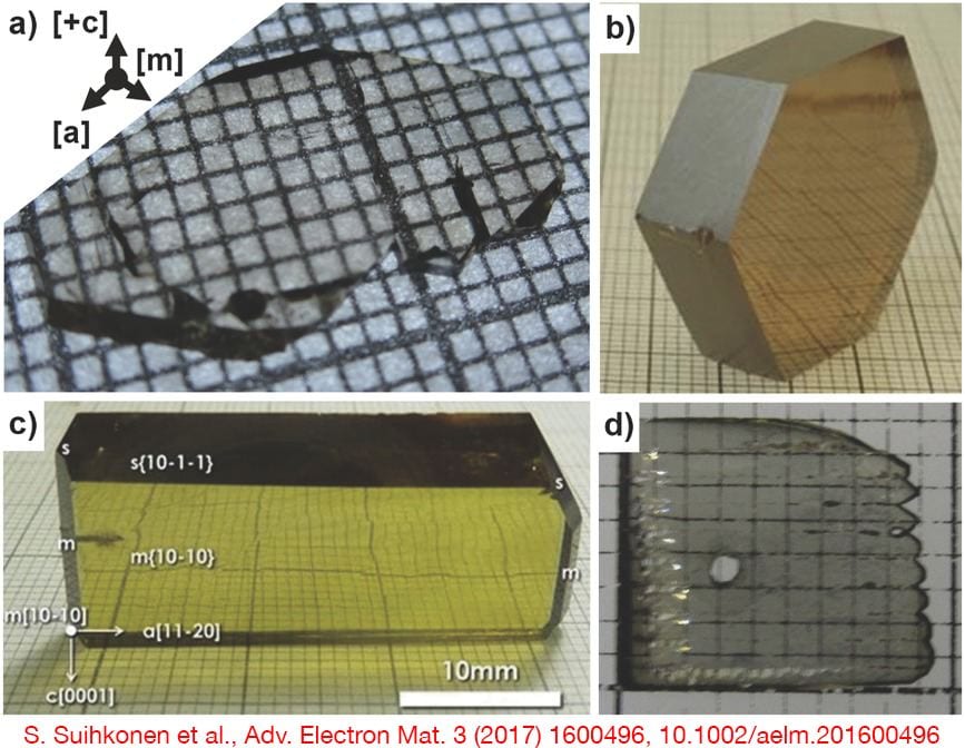
Native bulk gallium nitride (GaN) has emerged as an alternative for sapphire and silicon as a substrate material for III‐N devices. While quasi‐bulk GaN substrates are currently commercially available, single crystal GaN substrates are considered essential for future high performance light emitters and power devices. The ammonothermal method is currently considered one of the most feasible methods to grow large truly bulk crystals of GaN at low cost and high structural quality. High crystalline quality GaN substrates sliced from ammonothermally grown crystals have been demonstrated and utilized in homoepitaxy for III‐N devices. However, despite the high crystalline quality the properties of as‐grown ammonothermal GaN crystals and substrates are affected by the presence of impurities and other defects that hinder their use for device applications. Here, the main developments of ammonothermal growth of GaN and the effects of impurities, native point defects, and dislocations on the material properties are summarized. Additionally, measurement techniques that enable the evaluation of point defect concentration and low dislocation density distribution over a large area on bulk GaN substrates are reviewed. (Read full text)


